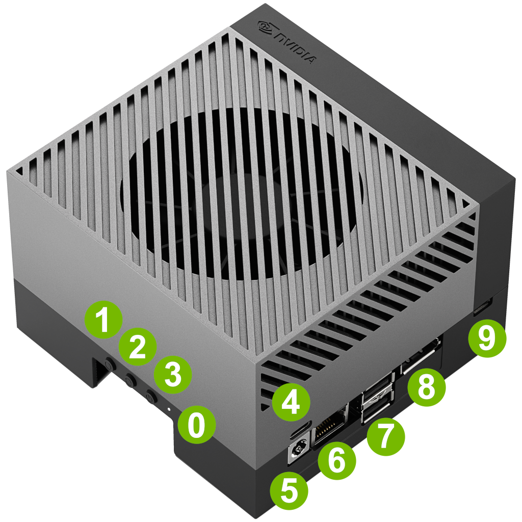
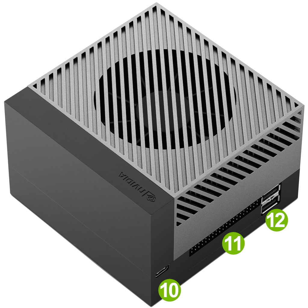
Hardware Layout#
Developer Kit#
Side Views#
 { .left }
 { .right }
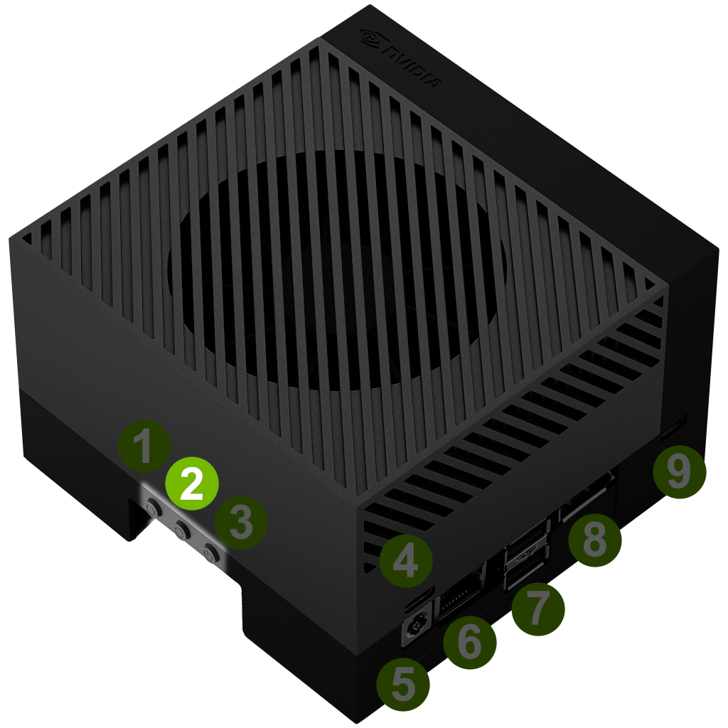
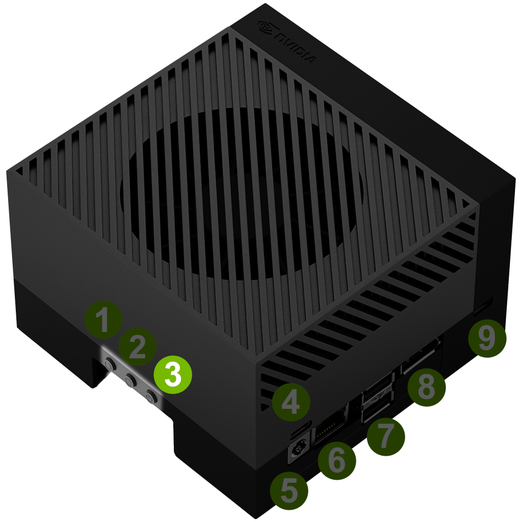
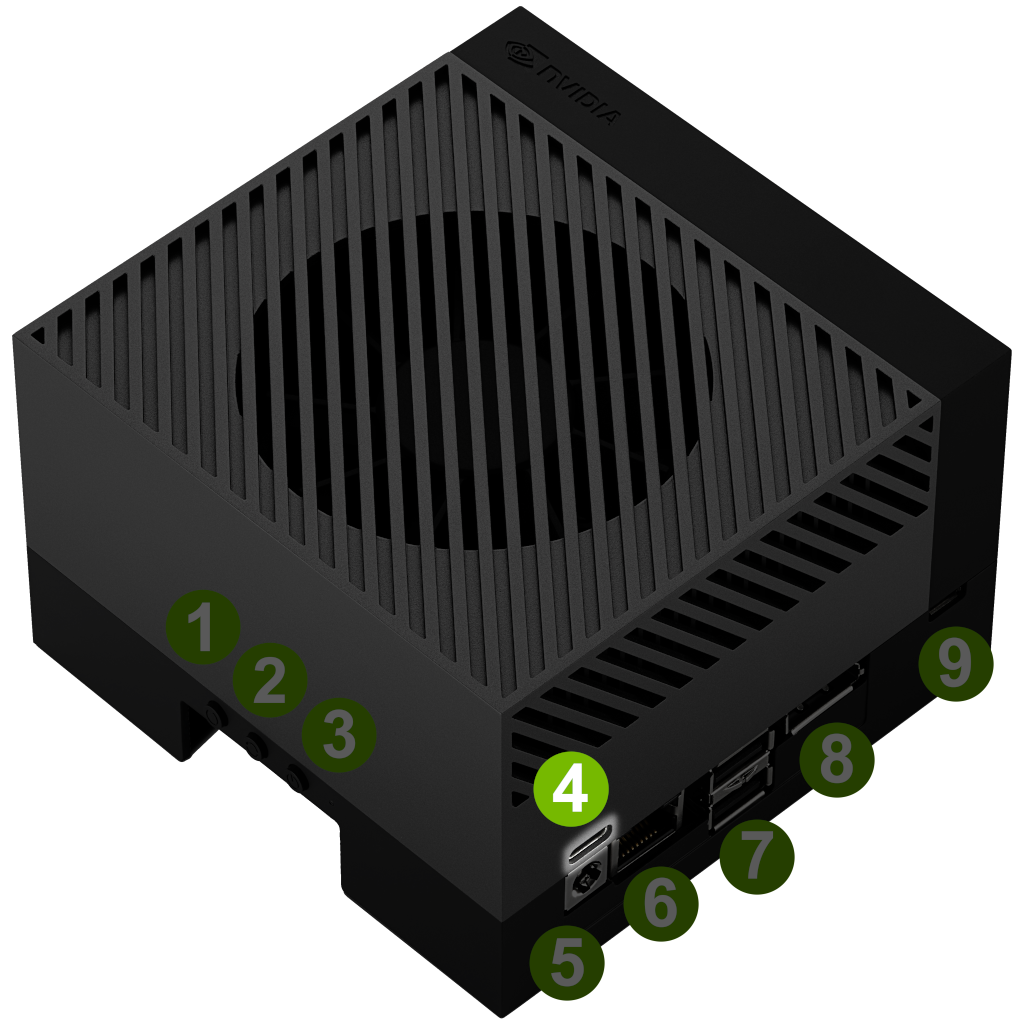
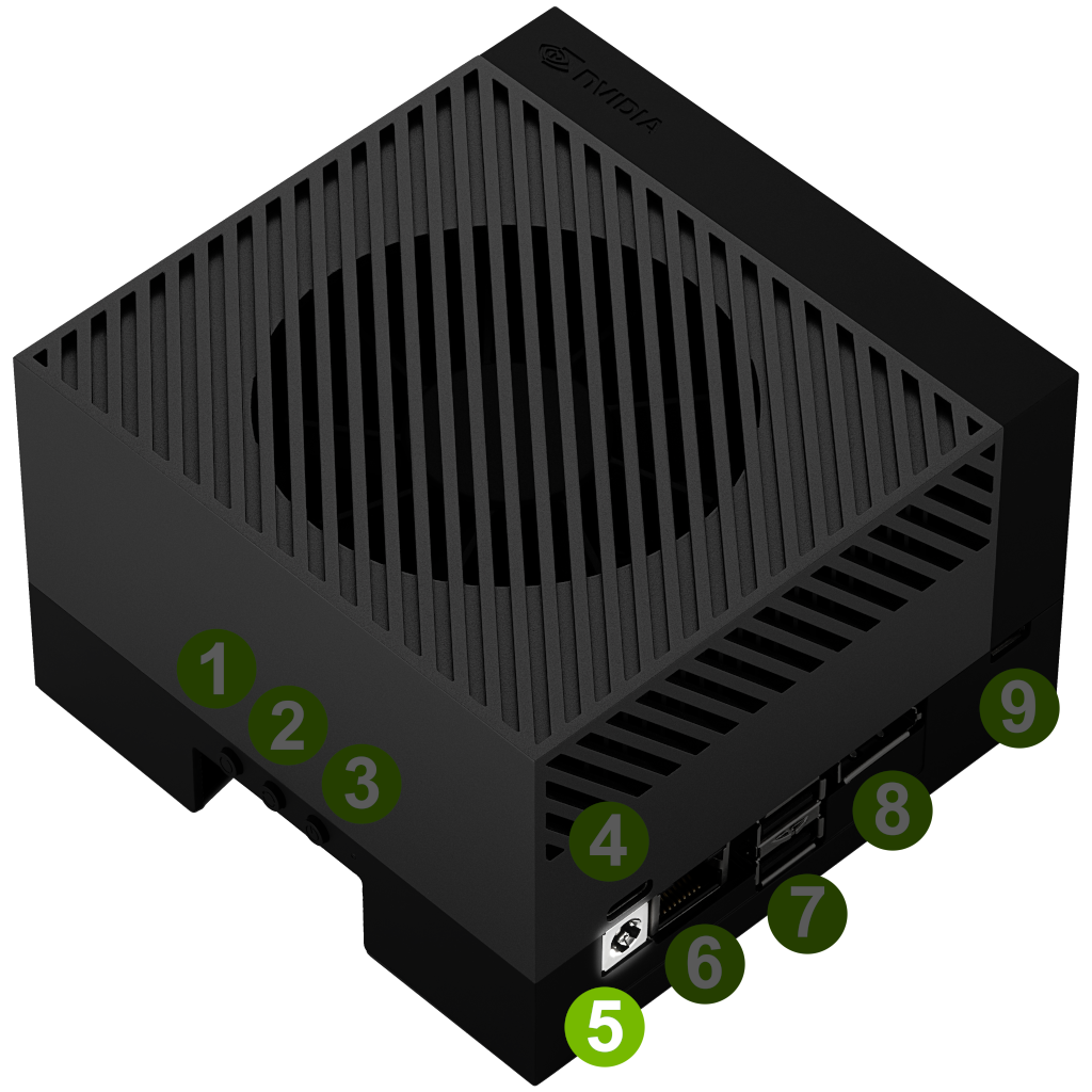
Part Names#
Mark. |
Name |
Note |
|---|---|---|
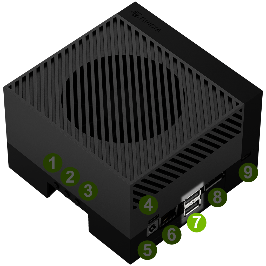
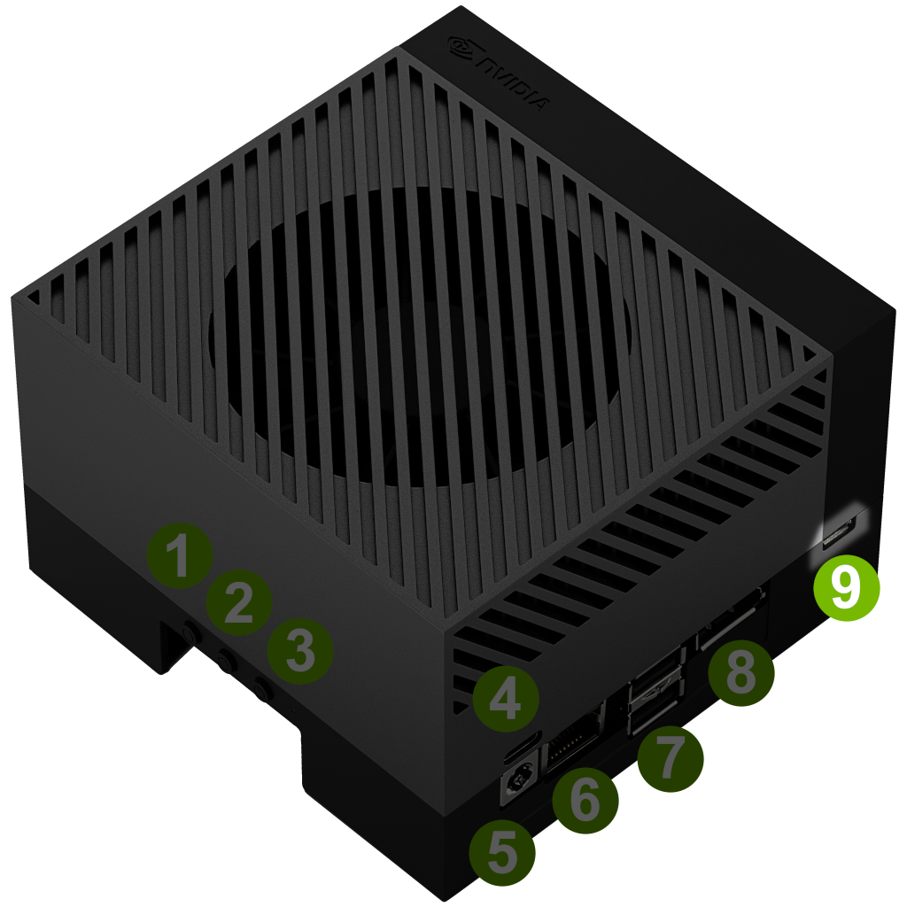
0 |
White LED |
|
1 |
Power button |
|
2 |
Force Recovery button |
|
3 |
Reset button |
|
4 |
USB Type-C port |
DFP only |
5 |
DC power jack |
|
6 |
Ethernet port |
|
7 |
USB Type-A ports |
2x USB 3.2 Gen 2 |
8 |
DisplayPort output |
This is the only display interface on Jetson AGX Orin Developer Kit |
9 |
USB micro-B port |
For debug |
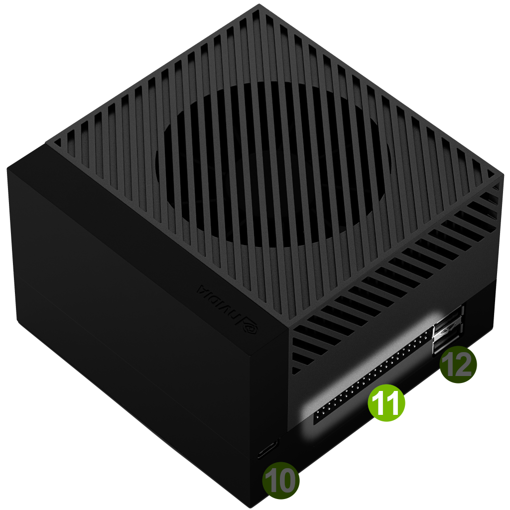
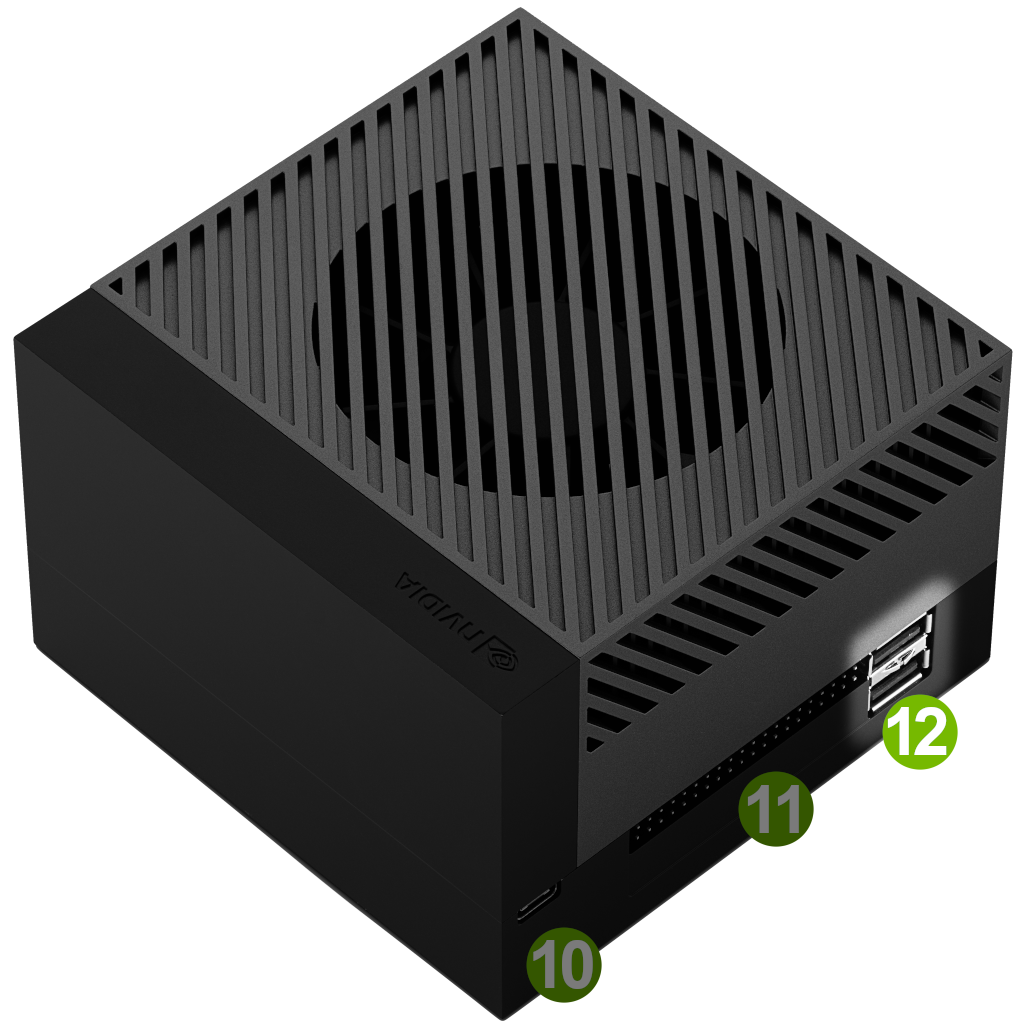
10 |
USB Type-C port |
Also for flashing (UFP and DFP) |
11 |
40-pin connector |
|
12 |
USB Type-A ports |
2x USB 3.2 Gen 1 |
Carrier Board#
!!! note
For the detail specification of the carrier board, see "[NVIDIA Jetson AGX Orin Developer Kit Carrier Board Specification](https://developer.nvidia.com/embedded/downloads#?search=Jetson%20AGX%20Orin%20Developer%20Kit%20Carrier%20Board%20Specification)".
Bottom View#
 { align=left }
 { align=left }
 { align=left }
 { align=left }
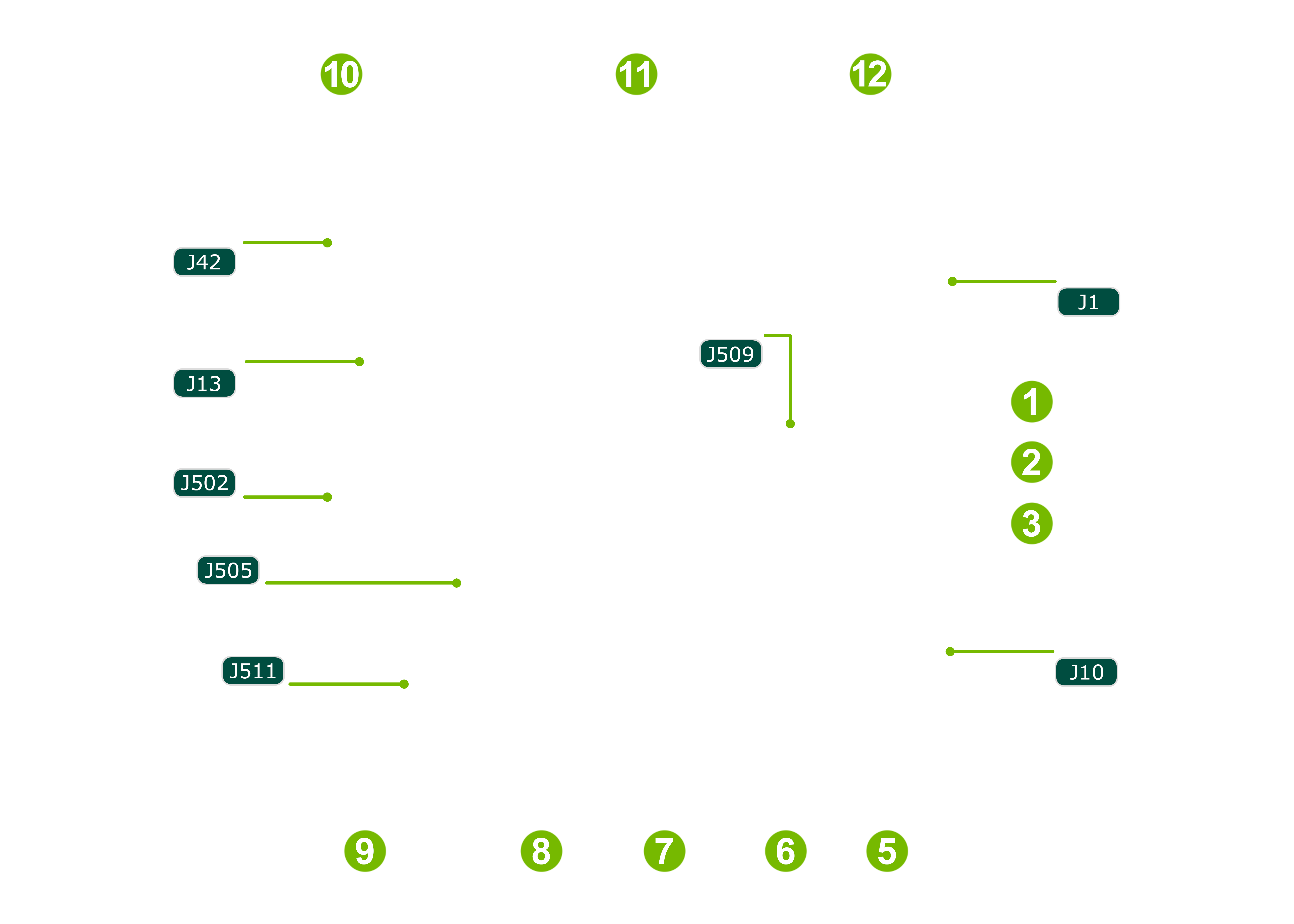
Part Names#
Mark. |
Name |
Specification |
|---|---|---|
0 |
White LED |
|
1 |
Power button |
|
2 |
Force Recovery button |
|
3 |
Reset button |
|
4 |
USB Type-C port (above DC power jack) |
DFP only, USB 3.2 Gen 2 |
5 |
DC power jack |
5.5 mm OD, 2.5mm ID, center positive |
6 |
Ethernet port |
Up to 10GBASE-T |
7 |
USB Type-A ports (next to Ethernet port) |
2x USB 3.2 Gen 2 |
8 |
DisplayPort output |
Supports MST |
9 |
USB micro-B port |
For Debug UART |
10 |
USB Type-C port (next to 40-pin header) |
UFP and DFP, USB 3.2 Gen 2 |
11 |
40-pin connector |
|
12 |
USB Type-A ports (next to 40-pin header) |
2x USB 3.2 Gen 1 |
J42 |
Automation header |
(Pin detail below) |
J13 |
RTC backup battery connector |
(compatible battery below) |
J509 |
Camera connector |
|
J502 |
JTAG Debug connector |
|
J505 |
M.2 E-Key slot |
|
J511 |
HD Audio header |
|
J1 |
M.2 M-Key slot |
|
J10 |
microSD card slot |
UHS-1 |
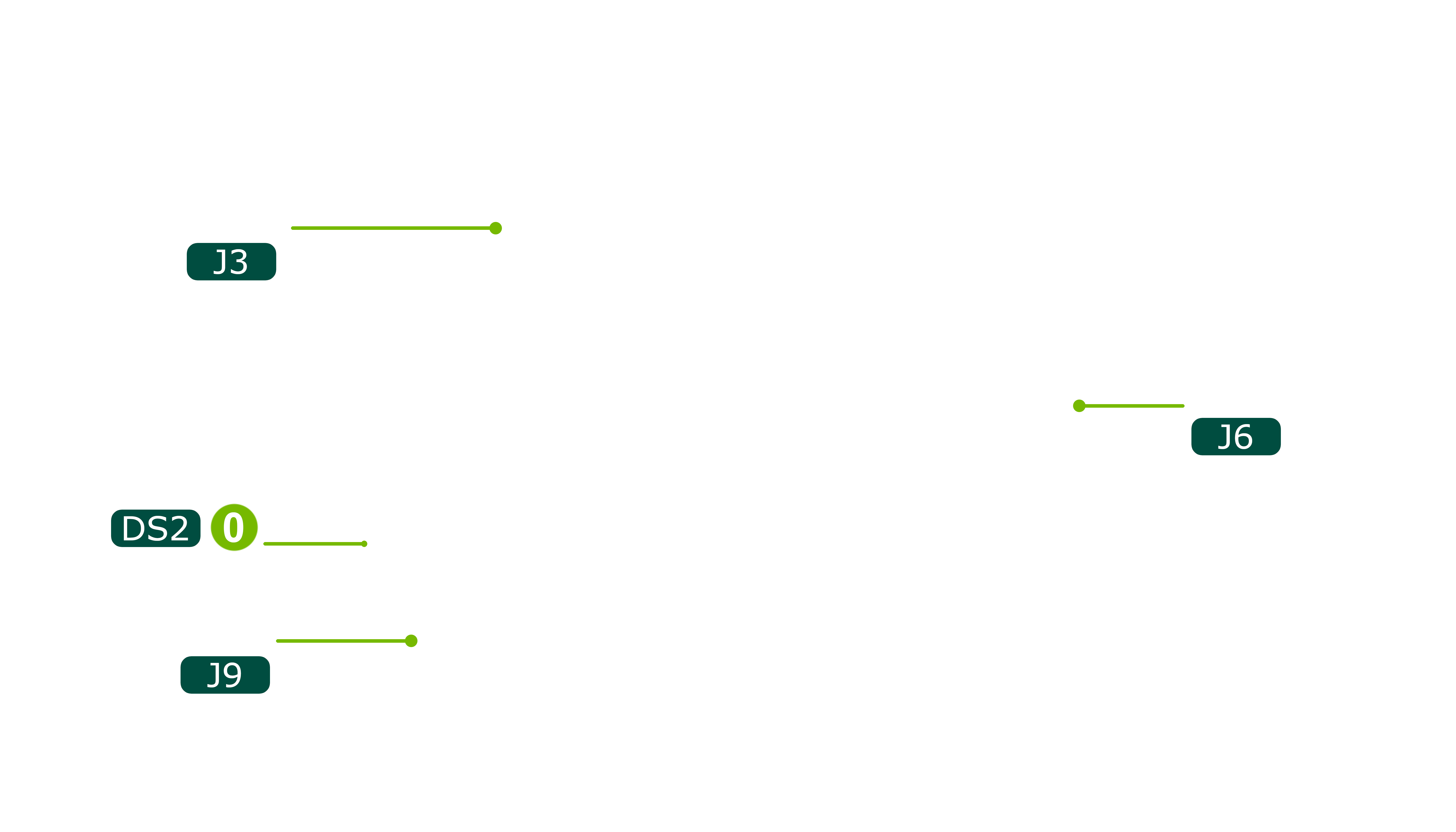
J3 |
Jetson module connector |
699 pin |
J6 |
PCIe x16 connector |
PCIe 4.0 x8 |
J9 |
Fan connector |
4-pin, 1.25mm pitch |
Miscellaneous Port and Connector Details#
!!! note
For the detail, see ["Jetson AGX Orin Developer Kit Carrier Board Specification"](https://developer.nvidia.com/embedded/downloads#?search=Jetson%20AGX%20Orin%20Developer%20Kit%20Carrier%20Board%20Specification).
DisplayPort Output#
To connect a display to the developer kit, use the DisplayPort output port ( 8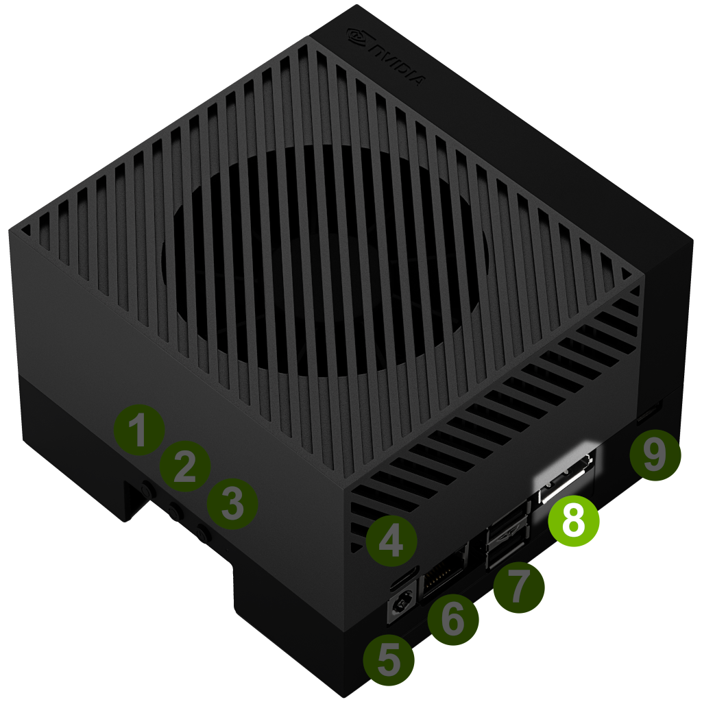 J18
J18 ). This is the only way to get the display out on the developer kit, the NVIDIA Jetson AGX Orin Developer Kit does not support HDMI or DisplayPort over USB-C.
To connect to a monitor or TV that only accepts HDMI, you can use an adaptor/cable that converts DisplayPort to HDMI.
DisplayPort output port supports;
DP SST
DP MST
Can support up to a max of 2 external displays
DP DSC
Max resolution (with or without DSC): 8k@30 / 4k@120
HBR3 / 4ln
Output Formats
RGB 8bpc
RGB 10bpc
YUV444 8bpc
YUV444 10bpc
Jetson Linux (L4T) r34.1.1 (packaged in JetPack 5.0.1 Developer Preview) and later supports passive DisplayPort to HDMI adapters. (Release Note)
Storage#
Default storage:
eMMC flash memory on the Jetson AGX Orin module.
Optional storage:
NVMe SSD card (on M.2 M-Key slot J1
USB thumb-drive (on any USB port).
microSD card (in microSD card slot J10
You can flash the base L4T BSP on to any of the storage medium above using SDK Manager.
See Step #5 of Use SDK Manager to Flash L4T BSP section on Software Setup with SDK Manager page
Ethernet port ( 6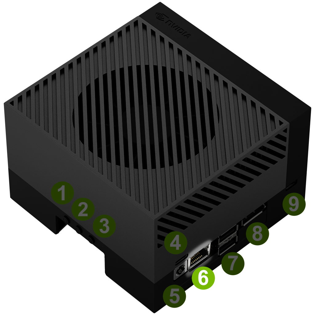 J17 )#
Indicator LED pattern:
Status & Speed |
Left side (SPEED LED) |
Right side (ACT LED) |
|---|---|---|
Connected |
|
Solid GREEN |
10M |
N/A |
N/A |
100M |
OFF |
Blinking GREEN |
1G |
YELLOW |
Blinking GREEN |
2.5G |
YELLOW |
Blinking GREEN |
5G |
YELLOW |
Blinking GREEN |
10G |
GREEN |
Blinking GREEN |
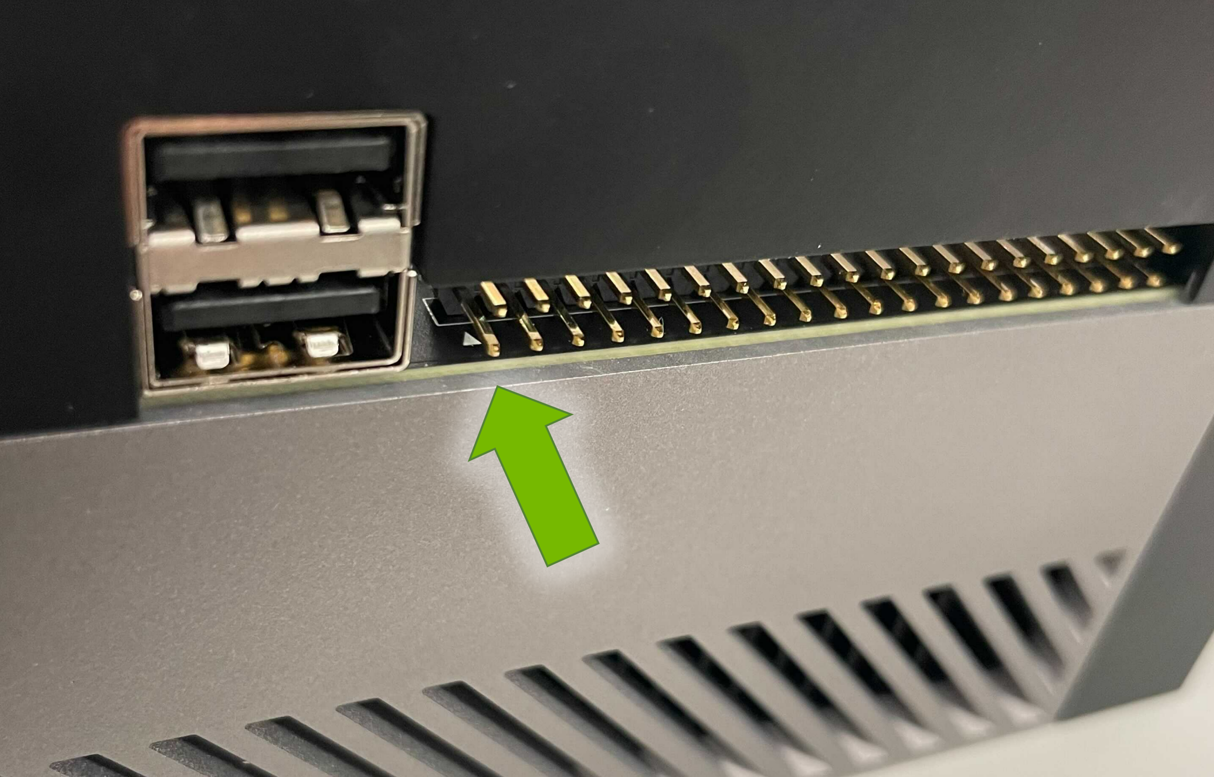
40-pin header ( 10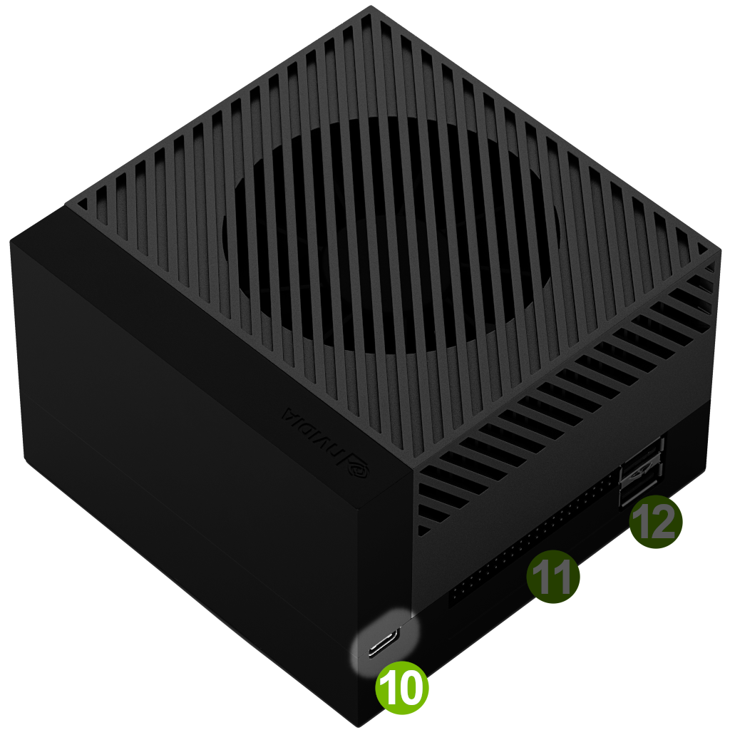 J40 )#
Pin assignment :


To identify the orientation of the 40-pin header (i.e. Pin 1), look for the white triangle marking on the PCB.
 { width=”500” }
For details, see NVIDIA Jetson AGX Orin Developer Kit Carrier Board Specification.
Automation header ( J42 )#
pin
#1,#12, GNDpin
#2,#3,#4: Input, same function as three buttons: Recovery, Reset, Power.pin
#5-#6: Open: Auto Power-On disable; Short: Auto Power-On enable.pin
#7: CVB_STBY: output, indicating module is in sleep or not.pin
#8: SYSTEM_OC: input, to trigger Tegra throttling.pin
#9-#10: Open: Wake(Boot) on LAN from Off state is disabled; Short: Wake(Boot) on Lan from Off state is enable.pin
#11: JTAG_TRST, JTAG Test Reset.
For details, see NVIDIA Jetson AGX Orin Developer Kit Carrier Board Specification.
RTC backup battery connector ( J13 )#
It can accommodate RTC backup battery with 1.25mm pitch connector, like these.
Camera connector ( J509 )#
MIPI CSI input (6x2/4x4 lane)
For detail, see NVIDIA Jetson AGX Orin Series Camera Module Hardware Design Guide .
HD Audio header ( J511 )#
This can be used to connect to a standard PC audio panel to support connections to microphone, line-in, headphones, powered speakers, etc.
For details, see NVIDIA Jetson AGX Orin Developer Kit Carrier Board Specification.
M.2 M-Key slot ( J1 )#
Supports 2280 size card, with PCIe x4 interface. No SATA support.
Jetson module connector ( J3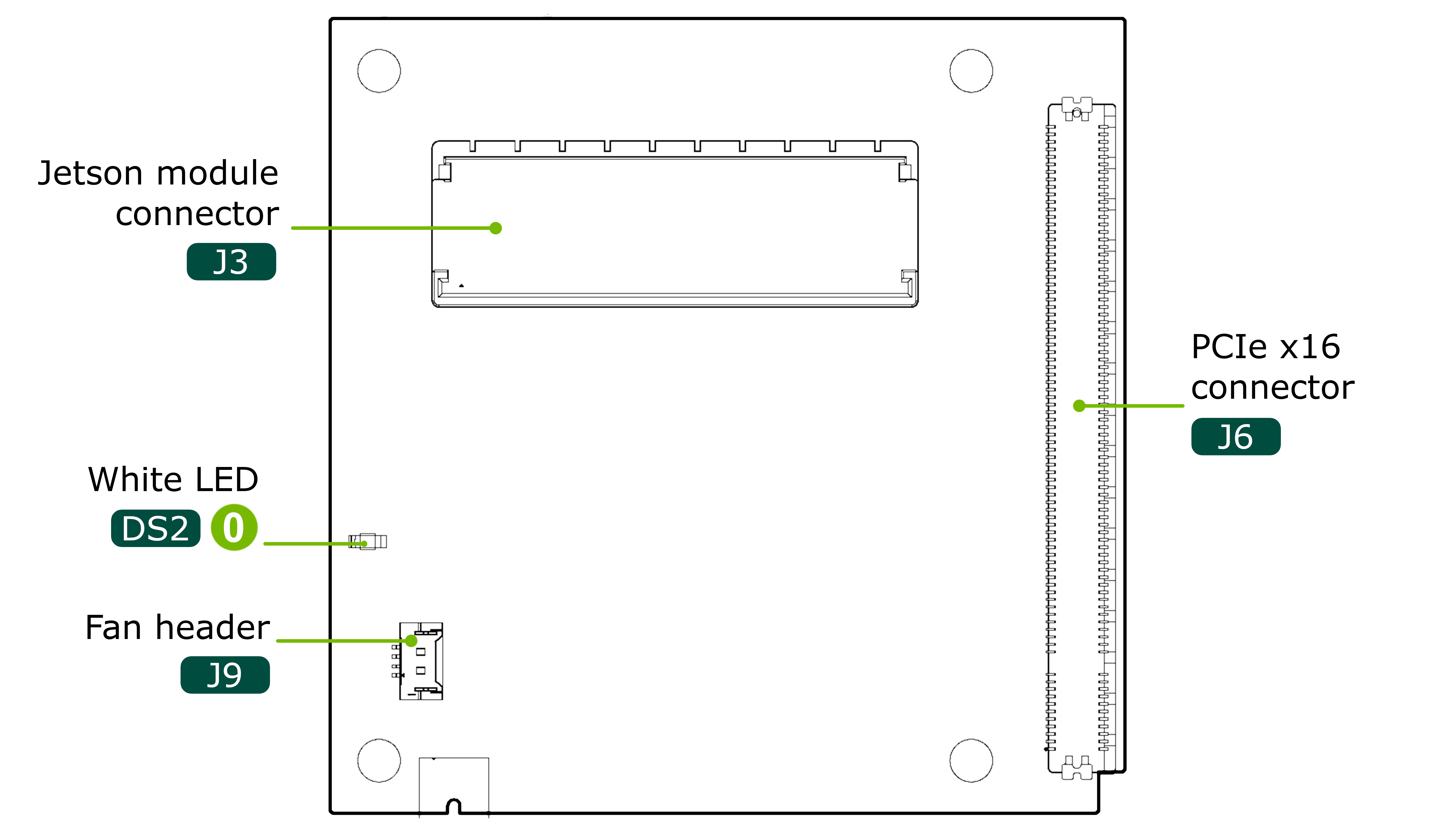 )#
)#
For detail, see Jetson AGX Orin Product Design Guide.
PCIe connector ( J6 )#
For verified PCIe cards, see Jetson AGX Orin Series Supported Component List.
To configure the PCIe interface as an Endpoint, see Jetson AGX Orin Series PCIe Endpoint Design Guidelines Application Note.