Jetson TX2 Series Adaptation and Bring-Up
This topic describes how to port NVIDIA® Jetson™ Linux Driver Package (L4T) and the U-Boot bootloader from NVIDIA® Jetson™ TX2 Developer Kit to another hardware platform.
This information applies to the following modules in the Jetson TX2 series:
• Original Jetson TX2
• Jetson TX2i (Industrial)
• Jetson TX2 4GB (with 4 GB of memory)
Jetson TX2 NX is not compatible with the carrier board in Jetson TX2 Developer Kit, and is described in the topic Jetson TX2 NX Adaptation and Bring-Up.
The examples described include code for the Jetson TX2 Developer Kit (P2771).
For information on customizing the configuration files, see the topics Jetson TX2 MB1 Platform Configuration.
Board Configuration
The Jetson TX2 module consists of a P3310 System on Module (SOM) connected to a P2597 carrier board. The part number P2771 designates the complete Jetson TX2 Developer Kit. The SOM can be used without any software configuration modifications. The SOM and carrier board each an EEPROM where the board ID is saved.
Before replacing the P2597 carrier board, verify the software programming of the Kernel device tables, MB1 configuration, ODM data, and flashing to de-configure the P2597 carrier board with the custom configurations of your custom board. EEPROM ID for your custom board is not required.
Board Naming
To support a Jetson TX2 module with your carrier board, you must assign the module/carrier board combination a lower case alphanumeric name. The name may include dashes (-) and underscores (_), but not spaces. Some examples of valid names are:
p2771-000-500
devboard
The name you select appears in:
• Filenames and pathnames
• U-Boot and Linux kernel source code
• User-visible device tree filenames
Additionally, this name is exposed to the user through the U-Boot command prompt and various Linux kernel proc files.
In this topic, <board> represents your board name.
You must also select a similarly-constructed vendor name. The same character set rules apply, such as the following example:
nvidia
In this topic, <vendor> represents your vendor name.
Note: | Do not re-use and modify the existing NVIDIA Jetson TX2 Developer Kit code without selecting and using your own board name. If you do not use your own board name it will not be obvious to Jetson TX2 users whether the modified source code supports the original Jetson TX2 Developer Kit board or your board. |
Placeholders in the Porting Instructions
Placeholders are used throughout this topic, substitute an appropriate value for each placeholder when executing commands.
• <function> is a functional module name, which may be power-tree, pinmux, sdmmc-drv, keys, comm (Wi-Fi/Bluetooth®), camera, etc.
• <board> is a name you have selected to represent your platform. For example, p2771 is the name of the Jetson TX2 Developer Kit. NVIDIA <board> names use lower case letters.
• <version> is a board version number, such as a00. Files for NVIDIA reference boards include a version number. Files for customer platforms are not required to include a version number.
• <vendor> is the name of your organization, or the name of the vendor for your board.
• <root> is the device that holds root file system for the platform. The supported value is emmc.
MB1 Configuration Changes
MB1 provides the boot time configuration of the hardware applied by the bootloader. The MB1 boot configuration tables are available at:
<l4t_top>/bootloader/t186ref/BCT
Pinmux Changes
If your board schematic differs from that for Jetson TX2 Developer Kit board, you must change the pinmux configuration applied by the software.
To define your board’s pinmux configuration, you must download the Jetson TX2 pinmux table from the Jetson Download Center and customize it for the configuration of your board using the following procedures.
The table is provided as a spreadsheet which:
• Shows the locations and default pinmux settings
• Defines the pinmux settings in the source code or device tree
The spreadsheet is available at:
You must customize the spreadsheet for the configuration of your board.
To customize the pinmux spreadsheet
1. Create a copy of the spreadsheet file with a name based on your board name, e.g. <board>_pinmux.xlsm. Note the directory in which you stored the copy; you will need it in the procedure Updating the Bootloader Pinmux.
2. Ensure that the new file is writable.
3. On a Windows PC, open the new file in Microsoft Excel.
4. If Microsoft Excel displays any warnings such as “PROTECTED VIEW” or “SECURITY WARNING,” click Enable Editing or Enable Content, so that you can save your changes to the new file.
5. Rename the Jetson-TX2-Config-Template tab based on the name of your board:
1. Right click the Jetson-TX2-Config-Template tab at the bottom of the window.
2. Click the Rename menu option.
3. Type your board name into the tab, then press ENTER.
6. Modify the spreadsheet columns grouped under the heading “Filled in by Customers” as required by the pinmux configuration for your board, based on the schematic.
7. Once the spreadsheet reflects the configuration you want, click the Generate DT File button to run a macro that exports the configuration data to a set of .dtsi files in the directory where the spreadsheet is stored. The macro prompts you to enter a prefix for the files’ names; enter jetson-tx2-default (the default).
To configure the pinmux setting of i2c-4 and i2c-6
You must make three changes to the device tree configure the pinmux settings of i2c-4 (dpaux1) and i2c-6 (dpaux0):
• In the i2c controller node, set pinctrl-0 to point to dpaux-default, and pinctrl-names to "default":
i2c@31b0000 {
pinctrl-names = "default";
pinctrl-0 = <&dpaux_default>;
};
• Define the dpaux controller node like this:
host1x {
dpaux@<nodename> {
status = "okay";
compatible = "nvidia,tegra186-dpaux-padctl";
dpaux_default: pinmux@0 {
dpaux_pins {
pins = "dpaux-<port>";
function = "i2c";
};
};
/delete-property/ power-domains;
};
};
Where:
• <nodename> is 155c0000 for dpaux0, or 15040000 for dpaux1
• <port> is "0" for depaux0. or "1" for dpaux1
For more information about this setting, see <TOP>/kernel/nvidia/Documentation/devicetree/bindings/pinctrl/nvidia,tegra186-dpaux-pinctrl.txt.
Updating the Bootloader Pinmux
The Jetson TX2 bootloader uses a .cfg file generated from the device tree files that you created in step 7 of To customize the pinmux spreadsheet.
The pinmux settings are only applied by the bootloader, and are not reapplied by the Linux kernel.
To update the bootloader pinmux
1. Determine the Jetson TX2 device tree version. You can determine the version from the device tree source file name, which can be found by executing this command on Jetson TX2:
$ cat /proc/device-tree/nvidia,dtsfilename
For example, if the file name is tegra186-quill-p3310-1000-c03-00-base.dts, the version is c03.
2. Enter the following commands:
$ cd Linux_for_Tegra/kernel/pinmux/t186/
$ python pinmux-dts2cfg.py --pinmux addr_info.txt gpio_addr_info.txt por_val.txt --mandatory_pinmux_file mandatory_pinmux.txt \
tegra18x-jetson-tx2-default-template-pinmux.dtsi \
tegra18x-jetson-tx2-default-template-gpio-default.dtsi 1.0 \
> ../../../bootloader/t186ref/BCT/tegra186-mb1-bct-pinmux-quill-p3310-1000-<version>.cfg
Where:
• If you specified a prefix other than the one recommended in step 7 of To customize the pinmux spreadsheet, substitute that prefix for jetson-tx2-default in the .dtsi files’ names.
These commands convert the .dtsi files generated in To customize the pinmux spreadsheet to a .cfg file and store it in the L4T release package at Linux_for_Tegra/kernel/pinmux/t186/.
3. To reflash the target device for the new pinmux configuration to be applied, follow the instructions in the section Basic Flashing Procedures of the topic Flashing and Booting the Target Device.
GPIO Changes
If you designed your own carrier board, to translate from SOM-connector pins to actual GPIO numbers you must understand GPIO mapping formula below. The translated GPIO numbers can be controlled by the driver.
For example, to check the GPIO number of GPIO15/AP2MDM_READY. perform the following steps.
To check the GPIO number
1. Search for GPIO15_AP2MDM_READY in Jetson_TX2_Generic_Customer_Pinmux_Release.xlsx.
2. Confirm that the Customer Usage field is applied to GPIO3_PBB.00.
3. Refer to tegra186-gpio.h to determine the GPIO group that the GPIO belongs to and the index of the GPIO in the group. For example, GPIO3_PBB.00 belongs to the main Jetson GPIO group, and its port number is 21:
#define TEGRA_MAIN_GPIO_PORT_BB 21
4. Because the SoC device registers GPIOs dynamically, you must search kernel messages to find the base index of each GPIO group. The command and resulting output are similar to:
$ sudo grep tegra-gpio /sys/kernel/debug/gpio
gpiochip1: GPIOs 256-319, parent: platform/c2f0000.gpio, tegra-gpio-aon:
gpiochip0: GPIOs 320-511, parent: platform/2200000.gpio, tegra-gpio:
In this example the output shows that the GPIO groups and their base indices are:
• tegra-gpio, at base index 320
• tegra-gpio-aon, at base index 256
5. Because PBB00 belongs to the tegra-gpio group, its base index is 320. Use the following formula to calculate the GPIO number:
TEGRA_MAIN_GPIO(port, base) = (base + (8 * port) + pin)
Hence, the GPIO number of GPIO15/AP2MDM_READY is 320+(8*21)+0 = 488
PMIC Changes
The PMIC configuration file configures the initial PMIC in the P3310 board. Some GPIO expander-based GPIO regulator settings in the P2597 carrier board configurations are also defined. Review this configuration file to replace any references to the P2597 carrier board to your custom board. If required, include any regulator information to enable this file.
For example, remove the following section that is writing to a slave on the I2C controller 0 address 0x74 in the P2597 carrier board. Additionally, update the number of blocks and array number for other entries of the block:
tegra186-mb1-bct-pmic-quill-p3310-1000-c04.cfg
# 5V0_HDMI_EN
pmic.generic.1.block[2].type = 1; # I2C Type
pmic.generic.1.block[2].i2c-controller-id = 0;
pmic.generic.1.block[2].slave-add = 0xE8; # 7BIt:0x74
pmic.generic.1.block[2].reg-data-size = 8;
pmic.generic.1.block[2].reg-add-size = 8;
pmic.generic.1.block[2].block-delay = 10;
pmic.generic.1.block[2].count = 2;
pmic.generic.1.block[2].commands[0].0x07.0xFF = 0xEF;
pmic.generic.1.block[2].commands[1].0x03.0xFF = 0x10;
Porting the Linux Kernel
It is assumed that you are using the P3310 SOM provided by NVIDIA and that it has not been modified; the eMMC, PMIC, and DDR are the same with the same routing of lines. The modifications you are making are for the carrier board that hosts all the peripherals. Consequently, based on the peripherals present on your carrier board, you can modify the .dts files by disabling/enabling the controllers and changing the supplies.
To port the kernel configuration code (the device tree) to your platform, modify one of the distributed configuration files to describe the design of your platform.
The configuration files available at:
<top>/hardware/nvidia/platform/t18x/
<top>/hardware_nvidia/soc/t18x
The final DTB file used is:
tegra186-quill-p3310-1000-a00-00-base.dts
By reading the above file, you see which other .dtsi files are referenced by include statements. Common .dtsi files that may be modified to reflect hardware design changes include:
Types of Changes | DTSI Filename or location |
Power supply changes | tegra186-quill-power-tree-p3310-1000-a00-00.dtsi |
Regulator parameter changes | tegra186-quill-spmic-p3310-1000-a00-00.dtsi |
Display panel and node changes | See the topic Display Configuration and Bringup for details. |
ODM data based feature configuration | tegra186-odm-data-plugin-manager.dtsi |
NVIDIA SOC controller state to enable/disable a controller | soc/t18x/kernel-dts/tegra186-soc/ |
Panels related .dts files | tegra/common/kernel-dts/panels/ |
Verify that no other .dts or .dtsi file, including these .dts files, overrides any changes you make.
As a best practice, create your own set of .dts files based on the Quill files already present. Rename your newly created files to the name of your board.
Note: | Use fdtdump or dtc to generate a .dts from the final .dtb file and check if your changes have taken effect. |
The command usage is as follows:
dtc -I dtb -O dts tegra186-quill-p3310-1000-a00-00-base.dtb > tegra186-quill-p3310-1000-a00-00-base.dts
fdtdump dts tegra186-quill-p3310-1000-a00-00-base.dtb > tegra186-quill-p3310-1000-a00-00-base.dts
Porting USB (Universal Serial Bus)
Jetson TX2 can support up to three SuperSpeed USB ports. In some implementations not all of these ports can be used because of UPHY lane sharing among PCIE, SATA, UFS, and XUSB. The Jetson P2597 carrier board is designed and verified for one USB3.0 port and one USB 2.0 OTG-compatible port. If you designed your own carrier board, verify the UPHY lane mapping and compatibility between P2597 and your custom board by consulting the NVIDIA team.
USB Structure
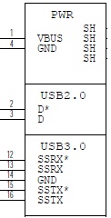
An enhanced SuperSpeed USB port has nine pins, as shown in the diagram below:
• VBUS
• GND
• D+
• D−
• Two differential signal pairs for SuperSpeed data transfer
• One ground (GND_DRAIN) for drain wire termination and managing EMI, RFI, and signal integrity
The D+/D− signal pins connect to UTMI pads. The SSTX/SSRX signal pins connect to UPHY and are handled by a single UPHY lane. As UPHY lanes are shared between PCIE, SATA, UFS, and XUSB, UPHY lanes must be assigned according to the custom carrier board’s requirements.
UPHY Lane Assignment
UPHY is an acronym for universal physical layer, a physical I/O interface layer that can serve multiple types of interfaces, e.g. USB, PCIe, SATA, and UFS. A UPHY lane can support multiple types of interfaces.
The Jetson P2597 carrier board is designed and verified for one USB3.0 port and one USB 2.0 OTG-compatible port. The possible use cases and their UPHY lane assignments are shown in the following table.
Config | Jetson TX2 Pin Names | PEX1/ USB_SS0 | PEX_RFU | PEX2 | USB_SS1 | PEX0 | SATA | |||
|---|---|---|---|---|---|---|---|---|---|---|
Jetson TX2 Lanes | Lane 0 | Lane 1 | Lane 3 | Lane 2 | Lane 4 | Lane 5 | ||||
Available Outputs from Jetson TX2 | ||||||||||
USB 3.0 | PCIe | SATA | ||||||||
1 | 0 | 1x1 + 1x4 | 1 | PCIe#2_0 | PCIe#0_3 | PCIe#0_2 | PCIe#0_1 | PCIe#0_0 | SATA | |
2 * | 1 | 1x4 | 1 | USB_SS#0 | PCIe#0_3 | PCIe#0_2 | PCIe#0_1 | PCIe#0_0 | SATA | |
3 | 2 | 3x1 ‡ | 1 | PCIe#2_0 | USB_SS#1 | PCIe#1_0 | USB_SS#2 | PCIe#0_0 | SATA | |
4 | 3 | 2x1 ‡ | 1 | USB_SS#0 | USB_SS#1 | PCIe#1_0 | USB_SS#2 | PCIe#0_0 | SATA | |
5 | 1 | 2x1 + 1x2 | 1 | PCIe#2_0 | USB_SS#1 | PCIe#1_0 | PCIe#0_1 | PCIe#0_0 | SATA | |
6 | 2 | 1x1 + 1x2 | 1 | USB_SS#0 | USB_SS#1 | PCIe#1_0 | PCIe#0_1 | PCIe#0_0 | SATA | |
* Configuration 2 represents the default on the carrier board. Lane 0 is assigned to USB SuperSpeed port 0, Lanes 1 through 4 are assigned to PCIe, and Lane 5 is assigned to SATA. † PCIe Interface 2 can be brought to the PEX1 pins, or USB 3.0 port 1 to the USB_SS0 pins, depending on the setting of a multiplexor on the module. The selection is controlled by QSPI_IO2 configured as a GPIO. To switch USB_SS0 to PEX1, configure QSPI_I02 as follows: pcie0_lane2_mux { gpio-hog; gpios = <TEGRA_MAIN_GPIO(R, 3) 0>; output-low; label = "pcie-lane2-mux"; - status = "disabled"; + status = "okay"; }; ‡ Although PCIe is 3x1 and 2x1 for configurations 3 and 4, the actual setting in the device tree must be x2, x1, x1. Otherwise pcie@1,0 does not work. pci@1,0 { nvidia,num-lanes = <2>; status = "okay"; } | ||||||||||
Jetson TX2 and the released software support all of the configurations described in the table above. However, the device tree and ODMDATA must be set to support the configuration you want to use. For further information, see the NVIDIA Jetson TX2 Technical Reference Manual (TRM). Consult with NVIDIA before designing your custom board.
Lane assignment can be defined by the uphy node in the bpmp-dtb file or by ODMDATA, defined in p2771-0000.conf.common. If both sources define lane assignment, the assignments in ODMDATA take priority.
If a customer device requires custom UPHY lane assignments, NVIDIA recommends defining them through ODMDATA because it can set related properties, such as MUX function properties, at the same time. You may prefer to perform lane assignment by modifying the bpmp-dtb file if you are thoroughly familiar with UPHY and UPHY lane assignment. Consult NVIDIA for further assistance if you are considering this.
bpmp-dtb
BPMP (Boot and Power Management Processor) is a Jetson TX2 processor that handles the boot process and offloads power management, clock management, and reset control tasks from the CPU. UPHY lane assignment is configured in the bpmp-dtb file under the device node uphy.
/ {
uphy {
lane0-owner = <TEGRA186_UPHY_LANE_XUSB>;
lane1-owner = <TEGRA186_UPHY_LANE_PCIE>;
lane2-owner = <TEGRA186_UPHY_LANE_PCIE>;
lane4-owner = <TEGRA186_UPHY_LANE_PCIE>;
lane5-owner = <TEGRA186_UPHY_LANE_SATA>;
};
};
ODMDATA and Plugin Manager
ODMDATA and Plugin Manager support special properties of various products’ device trees. While loading the BPMP firmware (BPMP-FW), Bootloader gets ODMDATA, checks the ODMDATA UPHY lane configuration bit, and updates the UPHY lane owners on bpmp-dtb. Later, BPMP-FW configures the UPHY lanes as defined by the updated DTB. This provides flexibility to maintain multiple board configurations during development
The following table shows the meanings of the ODMDATA bits that are related to UPHY lane assignment.
Bits | Name | Description |
|---|---|---|
31:29 | — | Reserved |
28 | UPHY_LANE5 | Each lane’s bits identify the function that owns the lane. Recognized values are: • 0: PCIE • 1: XUSB |
27 | UPHY_LANE4 | |
26 | UPHY_LANE2 | |
25 | UPHY_LANE1 | |
24 | UPHY_LANE0 | |
23:0 | — | Reserved |
For example:
• ODMDATA=0x1090000 while flashing for Jetson TX2 for configuration 2
• ODMDATA=0x90000 for configuration 1
• ODMDATA=0x6090000 for configuration 3
Required Device Tree Changes
This section gives step-by-step guidance for checking schematics and configuring USB ports in the device tree. All the examples are based on the design of Jetson TX2 P2597 carrier board.
For a Host-Only Port
This section uses J19, a USB 3.0 type A connector, as an example of a host-only port.
Go Through the Schematics
Note: | The P2597 carrier board’s schematic file, P2597_C02_Concept_schematics.pdf, is included in the Jetson TX1-TX2 Developer Kit Carrier Board Design Files, available at: |
Check the USB connectors on the P2597 carrier board and find the wired socket location to the P3310 module board.
• USB 2.0 signal pins D+/D- (DP and DN) wire out from J19 and lead to A39 (USB1_D) and A38 (USB1_D) on the module socket.

USB3.0 differential signal pairs (TX_* and RX_*) wire out from J19 and lead to C43 (USB_SS0_TX), C44 (USB_SS0_TX), F43 (USB_SS0_RX), and F44 (USB_SS0_RX) on the module socket.

• VBUS is enabled by USB_VBUS_EN1 which lead to A18 (USB1_EN_OC) on the module socket through U21, the USB power-distribution switch.

Through the schematic, we can conclude that for J19:
• The USB 2.0 signal pair is wired to UTMI pad 1 (USB2 port 1).
• The USB3.0 signal pairs are wired to UPHY lane 0 (USB3.0 port 0 according to UPHY lane mapping).
• The VBUS supply is controlled by USB1_EN_OC pin.
Under the Fixed-Regulators Node
The VBUS supply of the host driver (xHCI) is controlled with regulators. The device tree’s fixed-regulators node follows the conventions of the regulator.txt, fixed-regulator.txt, and gpio.txt kernel documents. The node’s properties are:
• compatible: If a regulator chip contains multiple regulators, and if the chip's binding contains a child node that describes each regulator, then this property indicates which regulator this child node configures. If this property is absent, the node's name is used instead.
Note: | The VBUS supply of J19 is controlled by the USB1_EN_OC GPIO pin. Hence compatible should be regulator-fixed-sync for fixed-regulator. |
• regulator-name: A string used as a descriptive name for regulator outputs.
• regulator-min-microvolt: Smallest voltage consumers may set, in microvolts. Must be "5000000".
• regulator-max-microvolt: Largest voltage consumers may set, in microvolts. Must be "5000000".
• gpio: The GPIO which enables and disables the regulator.
Take J19 USB3.0 type A connector for example. Create a pad and port nodes and property list for J19 based on the device tree structure described above:
fixed-regulators {
...
vdd_usb1_5v: regulator@5 {
compatible = "regulator-fixed-sync";
reg = <5>;
regulator-name = "vdd-usb1-5v";
regulator-min-microvolt = <5000000>;
regulator-max-microvolt = <5000000>;
gpio = <&tegra_main_gpio TEGRA_MAIN_GPIO(L, 5) 0>;
gpio-open-drain;
enable-active-high;
...
};
};
Note: | Check the pinmux table for the GPIO that corresponds to the USB1_EN_OC pin. |
Create the xusb_padctl Node
The device tree’s xusb_padctl node follows the conventions of the pinctrl-bindings.txt kernel document. It contains two groups named pads and ports, which describe USB2 and USB3 signals along with parameters and port numbers. The name of each parameter description subnode in pads and ports must be in the form <type>-<port_number>, where <type> is "usb2" or "usb3" and <port_number> is the associated port number.
The pads Subnode
The single property defined in the pads subnode is:
• nvidia,function: A string containing the name of the function to mux to the pin or group. Must be "xusb".
The ports Subnode
The properties defined in the ports subnode are:
• mode: A string that describes USB port capability. A port for USB2 must have this property. It must be one of the values "host", "device", or "otg".
• nvidia,usb2-companion: Specifies the USB2 port (0, 1, 2, or 3) to which the port is mapped. A port for USB3 must have this property.
• nvidia,oc-pin: Specifies the overcurrent VBUS pin the port is using. The value must be positive or zero.
• vbus-supply: The VBUS regulator for the corresponding UTMI pad. Set to "&battery_reg" for a dummy regulator.
For the detailed information about xusb_padctl, see the documentation at:
kernel/kernel-4.9/Documentation/devicetree/bindings/phy/nvidia,xusb-padctl.txt
Take J19 (a USB3.0 type A connector) as an example. Create pad and port nodes and property lists for J19 based on the device tree structure described above:
xusb_padctl: xusb_padctl@3520000 {
...
pads {
usb2 {
lanes {
usb2-1 {
nvidia,function = "xusb";
status = "okay";
};
...
};
};
usb3 {
lanes {
...
usb3-0 {
nvidia,function = "xusb";
status = "okay";
};
...
};
};
};
ports {
usb2-1 {
mode = "host";
vbus-supply = <&vdd_usb0_5v>;
status = "okay";
nvidia,oc-pin = <1>;
};
...
usb3-0 {
nvidia,usb2-companion = <1>;
status = "okay";
};
...
};
};
Create the xHCI Node
The Jetson TX2 xHCI controller complies with xHCI specifications, which support both USB 2.0 HighSpeed/FullSpeed/LowSpeed and USB 3.0 SuperSpeed protocols. The controller node’s properties are:
• phys: Must contain an entry for each entry in phy-names.
• phy-names: Must contain an entry for each PHY used by the controller. Names must be of the form <type>-<port_number>, where <type> is "usb2" or "usb3".
• nvidia,boost_cpu_freq: Specifies the value to which CPU frequency is boosted. This is only the minimum frequency; DVFS can scale up CPU frequency further based on need and CPU loading. CPU boost frequency through PMQOS is enabled for the xHCI controller only when this field’s value is greater than zero. The boost is applicable only for bulk and ISOC transfers; other endpoints do not need to be boosted.
• nvidia,boost_cpu_trigger: Minimum buffer length of the bulk or ISOC transfers beyond which to boost frequency.
• nvidia,xusb-padctl: A pointer to the xusb-padctl node.
For the detailed information about xHCI, see the documentation at:
kernel/kernel-4.9/Documentation/devicetree/bindings/usb/nvidia,tegra-xhci.txt
Take J19, a USB3.0 type A connector, as an example. Create an xHCI node and property list for J19 based on the device tree structure described above:
xhci@3530000 {
...
phys = <&{/xusb_padctl@3520000/pads/usb2/lanes/usb2-1}>,
<&{/xusb_padctl@3520000/pads/usb3/lanes/usb3-0}>;
phy-names = "usb2-1", "usb3-0";
nvidia,xusb-padctl = <&xusb_padctl>;
status = "okay";
...
};
For an OTG (On-The-GO) Compatible Port
USB On-The-Go, often abbreviated USB OTG or just OTG, is a specification that allows USB to act as a host or a device on the same port. A USB OTG port can switch back and forth between the roles of host and device.
Jetson TX2 USB supports OTG features when connected to a device that has an OTG port. For OTG feature support a fifth pin, the ID pin, is added to the standard USB connector.
An OTG cable has a type A plug on one end and a type B plug on the other end. The type A plug’s ID pin is grounded, while the type B plug’s ID pin is floating. A device with a type A plug inserted becomes an OTG type A device (a host), and a device with a type B plug inserted becomes a type B device (a client device).

Go Through the Schematics
Note: | The P2597 carrier board’s schematic file, P2597_C02_Concept_schematics.pdf, is included in Jetson TX2 Developer Kit Carrier Board Design Files, available at: |
Check the USB connectors on the P2597 carrier board and find the wired socket location to the P3310 module board.
• USB 2.0 signal pins D+/D− (DP and DN) wire out from J28 and lead to B40 (USB0_D) and B39 (USB0_D) on the module socket.

Note: | The OTG-compatible port, J28, only supports USB 2.0 and hence does not have USB 3.0 differential signal pairs on connector. |
• VBUS is enabled by USB_VBUS_EN0 which leads to A17 (USB0_EN_OC) on the module socket through U25, the USB power distribution switch.
• VBUS also wires out from J28 and leads to B37 (USB0_VBUS_DET) on the module socket as the VBUS_DETECT pin.
• The ID pin wires out from J28 and leads to A36 (USB0_OTG_ID) on the module socket.

Through the schematic, we can conclude that for J28:
• The USB 2.0 signal pair is wired to UTMI pad 0 (USB2 port 0).
• The VBUS supply is controlled by USB0_EN_OC pin.
• The VBUS pin is also wired to the USB0_VBUS_DET pin as the VBUS_DETECT pin.
• The ID pin is wired to the USB0_OTG_ID pin
Under the fixed-regulators Node
The fixed-regulators settings for an OTG-compatible port are the same as for a host-only port.
Take J28 USB 2.0 micro B connector as example. Create a fixed-regulators node and property list for J19 based on the device tree structure described above:
fixed-regulators {
...
vdd_usb0_5v: regulator@4 {
compatible = "regulator-fixed-sync";
reg = <4>;
regulator-name = "vdd-usb0-5v";
regulator-min-microvolt = <5000000>;
regulator-max-microvolt = <5000000>;
gpio = <&tegra_main_gpio TEGRA_MAIN_GPIO(L, 4) 0>;
gpio-open-drain;
enable-active-high;
...
};
};
Note: | Check the pinmux table for the GPIO that corresponds to the USB0_EN_OC pin. |
Under the xusb_padctl Node
The xusb_padctl settings for an OTG-compatible port are the same as for a host-only port except that the mode should be "otg".
Taking J28, the USB 2.0 micro-B connector, as an example, create pad and port nodes and property lists:
xusb_padctl: xusb_padctl@3520000 {
...
pads {
usb2 {
lanes {
usb2-0 {
nvidia,function = "xusb";
status = "okay";
};
...
};
};
...
};
ports {
usb2-0 {
mode = "otg";
vbus-supply = <&vdd_usb0_5v>;
status = "okay";
};
...
};
};
Under the extcon Node
External connectors, which may have different types of cables attached (USB, TA, HDMI, analog A/V, and others), often have device drivers that detect state changes at the port, and separate device drivers that do something according to the state changes.
The External Connector Class (extcon), introduced in 2012, supports the use of a notifier for passing information such as state changes between device drivers.
Generally, port switching between OTG roles is controlled by the host driver (xHCI) and device driver (xUDC), and can be defined by the state of the ID pin and the VBUS_DETECT pin.
Taking J28, the USB 2.0 micro B connector, as an example, the USB0_VBUS_DET GPIO pin acts as the VBUS_DETECT pin and USB0_OTG_ID as the ID pin, for example:
1. Find the corresponding GPIO states on the VBUS_DETECT pin and ID pin.
Generally, the ID pin is designed as internal pull high (logical high). With a type A plug connected the ID pin is pulled to ground (logical low), while with a type B plug connected or no cable connected it remains logical high.
The operation of the VBUS_DETECT pin depends on the device’s design. Consider the schematic of USB 2.0 micro B connector J28, for example.
VBUS_DETECT with a type B plug connected is logical low, because VBUS is provided from an external power supply. When no cable is connected it is logical high.
Note: | VBUS_DETECT is initially logical high, then logical low because VBUS is provided by the host controller. Therefore, the state of the VBUS_DETECT pin does not matter when the OTG-compatible port is operating in host mode. |
2. Create the table of GPIO states and their corresponding output cable states:
USB0_OTG_ID | USB0_VBUS_DET | EXTCON_STATE |
|---|---|---|
1 | 1 | 0x0 (EXCON_NONE) |
0 | 0 | 0x2 (EXTCON_USB_HOST) |
0 | 1 | 0x2 (EXTCON_USB_HOST) |
1 | 0 | 0x1 (EXTCON_USB) |
3. Create an extcon device node and property list based on the device tree structure.
Port switching between OTG roles is controlled by the state of the ID pin and the VBUS_DETECT pin and the settings of the external connector class. The node’s properties are:
• compatible: Value must be "extcon-gpio-states".
• extcon-gpio,name: Name of the extcon device.
• gpios: List of the GPIOs.
• extcon-gpio,irq-flags: IRQ flags for GPIO.
• extcon-gpio,debounce: Debounce time in milliseconds.
• extcon-gpio,wait-for-gpio-scan: Wait timeout in milliseconds for scanning all GPIOs’ states after a GPIO state change is detected and debounce time has passed.
• extcon-gpio,out-cable-names: Output cable names.
• extcon-gpio,cable-states: GPIO states and their corresponding output cable states. The value is an array of byte values. Each even-numbered byte is a GPIO state, and the following odd-numbered byte is the corresponding output cable state.
• cable-connected-on-boot: Name of the output cable connected on boot, expressed as an index into extcon-gpio,out-cable-names. The first element is index 0, and so on. If not specified, the system assumes that no cable is to be connected. This property is valid if no GPIOs are provided for cable states.
• wakeup-source: A Boolean; true if the device can wake up the system.
For detailed information about extcon, see the documentation at:
kernel/kernel-4.9/Documentation/devicetree/bindings/extcon/extcon-gpio-states.txt
Create an extcon device node and property list based on the device tree structure described above and the table of GPIO states and corresponding output cable states for the USB0_OTG_ID pin and the USB0_VBUS_DET pin:
vbus_id_extcon: usb_otg {
compatible = "extcon-gpio-states";
extcon-gpio,name = "VBUS_ID";
extcon-gpio,wait-for-gpio-scan = <0>;
extcon-gpio,cable-states = <0x3 0x0
0x0 0x2
0x1 0x2
0x2 0x1>;
gpios = <&tegra_main_gpio TEGRA186_MAIN_GPIO(X, 7) 0 &spmic 0 0>;
extcon-gpio,out-cable-names =
<EXTCON_USB EXTCON_USB_HOST EXTCON_NONE>;
wakeup-source;
#extcon-cells = <1>;
};
Note: | Check the pinmux table for the GPIO that corresponds to the USB0_OTG_ID and USB0_VBUS_DET pins. |
Under the xHCI Node
The xHCI settings for an OTG-compatible port are the same as for a host-only port except for the addition of extcon settings:
• extcon-cables: OTG-compatible support. Must contain a pointer to the excon-cable entry for the USB ID pin. When the extcon cable state is 0, the OTG-compatible port transitions to host mode.
• extcon-cable-names: Must be "id".
• #extcon-cells: Number of cells in the extcon specifier. Must be 1.
Taking J28, the USB 2.0 micro-B connector, as an example, create an xHCI node and property list based on the device tree structure described in Create the xHCI Node for a host-only port, plus the extcon settings above:
xhci@3530000 {
...
extcon-cables = <&vbus_id_extcon 1>;
extcon-cable-names = "id";
#extcon-cells = <1>;
phys = <&{/xusb_padctl@3520000/pads/usb2/lanes/usb2-0}>;
phy-names = "usb2-0";
nvidia,xusb-padctl = <&xusb_padctl>;
status = "okay";
...
};
Under the xUDC Node
The Jetson TX2 xUDC controller supports both USB 2.0 HighSpeed/FullSpeed and USB 3.0 SuperSpeed protocols.
• extcon-cables: OTG featire support. Must contains an excon-cable entry which detects USB VBUS pin. When the extcon cable state is 1, OTG-compatible port transitions to device mode.
• extcon-cable-names: Must be "vbus".
• charger-detector: USB charger detection support. Must be the phandle of the USB charger detection driver DT node.
• phys: An array; must contain pointers to the nodes that define each PHY in phy-names.
• phy-names: An array; must contain entries for each PHY used by the controller. Names must be in the form <type>-<port_number>, where <type> is one of "usb2" or "usb3".
• nvidia,boost_cpu_freq: The value to which CPU frequency is to be boosted. This is only the minimum frequency; DVFS can scale up CPU frequency further based on need and CPU load. CPU boost frequency through PMQOS is enabled for the xUDC controller only when this field’s value is greater than zero. The boost is applicable only to large bulk transfers on bulk endpoints; other endpoints do not need to be boosted.
• nvidia,xusb-padctl: Must be a pointer to the xusb-padctl node.
For the detailed information about xUDC, see the documentation at:
kernel/kernel-4.9/Documentation/devicetree/bindings/pinctrl/nvidia,tegra186-xudc.txt
Taking J28, the USB 2.0 micro B connector, as an example, create an xUDC node and property list for J28 based on the device tree structure described above:
xudc@3550000 {
extcon-cables = <&vbus_id_extcon 0>;
extcon-cable-names = "vbus";
#extcon-cells = <1>;
phys = <&{/xusb_padctl@3520000/pads/usb2/lanes/usb2-0}>;
phy-names = "usb2";
nvidia,xusb-padctl = <&xusb_padctl>;
nvidia,boost_cpu_freq = <1200>;
status = "okay";
};
USB Lane Mapping Issues
If you suspect a UPHY lane mapping issue, check the lane assignments programmed by BPMB firmware, based on ODMDATA:
4. UPHY lane 0: ./devmem2 0x02520284
5. UPHY lane 1: ./devmem2 0x02530284
6. UPHY lane 2: ./devmem2 0x02540284
7. UPHY lane 3: ./devmem2 0x02550284
8. UPHY lane 4: ./devmem2 0x02560284
9. UPHY lane 5: ./devmem2 0x02570284
Bits 0‒2 identify the function that owns the lane:
• 0x00: XUSB
• 0x01: PCIe
• 0x02: SATA
If a target UPHY lane is not owned by the correct function, check the value of ODMDATA that was flashed to be sure that the target lane was assigned correctly.
Check the device tree values used at runtime to ensure that Plugin Manager did not override them unexpectedly.
For example, confirm that the proper properties are enabled by running the command:
ls /proc/device-tree/chosen/plugin-manager/odm-data/
For a custom board, configure ODMDATA properly and check all the values. This example shows the values under listed from /proc/device-tree/chosen/plugin-manager/odm-data/, which represent the properties generated from ODMDATA, for a Jetson TX2 P2597 carrier board:
android-build enable-denver-wdt enable-xusb-on-uphy-lane0
disable-pmic-wdt enable-pcie-on-uphy-lane1 name
disable-sdmmc-hwcq enable-pcie-on-uphy-lane2 no-battery
disable-tegra-wdt enable-pcie-on-uphy-lane4 normal-flashed
enable-debug-console enable-sata-on-uphy-lane5
Note: | Before designing your custom board, verify the lane mapping by consulting Jetson TX2 OEM Product Design Guide, available at: |
Removing the DRAM ECC Partition
Applies to: Jetson TX2 series only
ECC DRAM is present only on NVIDIA® Jetson™ TX2i, but the default flashing partition layout reserves regions for ECC support on all NVIDIA Jetson™ TX2 series processors. If you are using another member of the Jetson TX2 series and you want to remove these regions to save secondary storage, perform these steps:
1. Edit bootloader/t186ref/BCT/tegra186-mb1-bct-misc-si-l4t.cfg relative to the flashing directory and set these two flags:
enable_blacklisting = 0;
disable_staged_scrub = 1;
2. Edit bootloader/t186ref/cfg/flash_l4t_t186.xml relative to the flashing directory, and remove these partitions:
• DRAMECCNAME
• BADPAGENAME
• BADPAGENAME_b
Flashing the Build Image
When flashing the build image, use your specific board name. The flashing script uses the configuration present in the <board>.conf file during the flashing process.
Setting Optional Environment Variables
The flash.sh script updates the following environment variables based on board EEPROM values and other parameters. If you want to override these environment variables’ default values, set them in the board-specific file board.conf.
# Optional Environment Variables:
# BCTFILE ---------------- Boot control table configuration file to be used.
# BOARDID ---------------- Pass boardid to override EEPROM value
# BOARDREV --------------- Pass board_revision to override EEPROM value
# BOARDSKU --------------- Pass board_sku to override EEPROM value
# BOOTLOADER ------------- Bootloader binary to be flashed
# BOOTPARTLIMIT ---------- GPT data limit. (== Max BCT size + PPT size)
# BOOTPARTSIZE ----------- Total eMMC HW boot partition size.
# CFGFILE ---------------- Partition table configuration file to be used.
# CMDLINE ---------------- Target cmdline. See help for more information.
# DEVSECTSIZE ------------ Device Sector size. (default = 512Byte).
# DTBFILE ---------------- Device Tree file to be used.
# EMMCSIZE --------------- Size of target device eMMC (boot0+boot1+user).
# FLASHAPP --------------- Flash application running in host machine.
# FLASHER ---------------- Flash server running in target machine.
# INITRD ----------------- Initrd image file to be flashed.
# KERNEL_IMAGE ----------- Linux kernel zImage file to be flashed.
# MTS -------------------- MTS file name such as mts_si.
# MTSPREBOOT ------------- MTS preboot file name such as mts_preboot_si.
# NFSARGS ---------------- Static Network assignments.
# <C-ipa>:<S-ipa>:<G-ipa>:<netmask>
# NFSROOT ---------------- NFSROOT i.e. <my IP addr>:/exported/rootfs_dir.
# ODMDATA ---------------- Odmdata to be used.
# PKCKEY ----------------- RSA key file to use to sign bootloader images.
# ROOTFSSIZE ------------- Linux RootFS size (internal emmc/nand only).
# ROOTFS_DIR ------------- Linux RootFS directory name.
# SBKKEY ----------------- SBK key file to use to encrypt bootloader images.
# SCEFILE ---------------- SCE firmware file such as camera-rtcpu-sce.img.
# SPEFILE ---------------- SPE firmware file path such as bootloader/spe.bin.
# FAB -------------------- Target board's FAB ID.
# TEGRABOOT -------------- lowerlayer bootloader such as nvtboot.bin.
# WB0BOOT ---------------- Warmboot code such as nvtbootwb0.bin
Note: | All the parameters must be added below the reference to the file <xxx>.conf.common to be reflected in the flashed image. |
Here is an example of environment variable settings:
source "${LDK_DIR}/p2771-0000.conf.common";
PINMUX_CONFIG="tegra186-mb1-bct-pinmux-quill-p3310-1000-a00.cfg";
BPFDTB_FILE=tegra186-a02-bpmp-quill-p3310-1000-a00-00-te770d-ucm2.dtb;
DTB_FILE=tegra186-quill-p3310-1000-a00-00-edp.dtb;
TBCDTB_FILE=tegra186-quill-p3310-1000-a00-00-edp.dtb;
EMMC_BCT="P3310_A00_8GB_Samsung_8GB_lpddr4_204Mhz_A02.cfg";
MISC_COLD_BOOT_CONFIG="tegra186-mb1-bct-misc-si.cfg";
To flash the build image
• Execute the following command.
$ sudo ./flash.sh <board> mmcblk0p1