Jetson AGX Xavier Series Adaptation and Bring-Up
This topic describes how to port NVIDIA® Jetson™ Linux (L4T) from NVIDIA® Jetson AGX Xavier™ Developer Kit to another hardware platform. It applies to all modules that are members of the Jetson AGX Xavier series:
• P2888-0001: Jetson AGX Xavier (16 GB memory)
• P2888-0004: Jetson AGX Xavier (32 GB memory)
• P2888-0005: Jetson AGX Xavier 64GB (64 GB memory)
• P2888-0008: Jetson AGX Xavier Industrial
The examples described include code for the Jetson AGX Xavier Developer Kit (P2972).
For information on customizing the configuration files, see the topics Jetson Xavier NX Series and Jetson AGX Xavier Series MB1 Platform Configuration.
Board Configuration
Jetson AGX Xavier Developer Kit consists of a P2888 System on Module (SOM) connected to a P2822 (B03 revision) carrier board. Part number P2972 designates the complete Jetson AGX Xavier Developer Kit. The SOM and carrier board each have an EEPROM where the board ID is saved. The SOM can be used without any software configuration modifications.
The SOM sold for incorporation into customer products has a Thermal Transfer Plate (TTP) ready to accept a customer-provided thermal solution. The module shipped as part of the Developer Kit has no TTP; instead it has a thermal solution designed specifically for the Developer Kit. This thermal solution must not be removed from the module.
Before using the SOM with a carrier board other than P2822, change the kernel device tree, MB1 configuration, ODM data, and flashing configuration to include configuration for the new carrier board instead of for P2822. EEPROM ID for your custom board is not required.
Board Naming
To support a Jetson AGX Xavier module with your carrier board, you must assign the module/carrier board combination a lower case alphanumeric name. The name may include hyphens (-) and underscores (_), but not spaces. Some examples of valid names are:
p2972-0000-devkit
devboard
The name you select appears in:
• Filenames and pathnames
• User-visible device tree filenames
Additionally, this name is exposed to the user through various Linux kernel proc files.
In this topic, <board> represents your board name.
You must also select a similarly-constructed vendor name. The same character set rules apply, such as the following example:
nvidia
In this topic, <vendor> represents your vendor name.
Note: | Do not re-use and modify the existing NVIDIA Jetson AGX Xavier Developer Kit code without selecting and using your own board name. If you do not use your own board name it will not be obvious to Jetson AGX Xavier series users whether the modified source code supports the original Jetson AGX Xavier Developer Kit board or your board. |
Placeholders in the Porting Instructions
Placeholders are used throughout this topic, substitute an appropriate value for each placeholder when executing commands.
• <function> is a functional module name, which may be power-tree, pinmux, sdmmc-drv, keys, comm (Wi-Fi/Bluetooth®), camera, etc.
• <board> is a name you have selected to represent your platform. For example, P2972 is the name of the Jetson AGX Xavier Developer Kit. NVIDIA <board> names use lower case letters.
• <version> is a board version number, such as a00. Files for NVIDIA reference boards include a version number. Files for customer platforms are not required to include a version number.
• <vendor> is the name of your organization, or the name of the vendor for your board.
• <root> is the device that holds root file system for the platform. The supported value is emmc.
Camera Connector Pin Differences
The table below describes camera connector pin differences between Jetson AGX Xavier series modules and the earlier NVIDIA® Jetson™ TX1 and Jetson TX2 modules.
In summary, a Jetson AGX Xavier module:
• Adds four additional CSI lanes and places CSI6 where CSI5 was. CSI5 moves to where UART and DMIC were
• Removes the 1.2V and 5V rails (or changes 5V to 3.3V)
• Removes UART, SPI, DMIC, and I2S
• Removes Flash, Auto-Focus, and Strobe Control
• Removes Motion Int and Modem to AP Ready
Pin | Jetson TX1/TX2 | Jetson AGX Xavier series | Notes |
|---|---|---|---|
1 | CSI0 | CSI0 | Equivalent |
2 | CSI1 | CSI1 | Equivalent |
3 | CSI0 | CSI0 | Equivalent |
4 | CSI1 | CSI1 | Equivalent |
5 | GND | GND | Equivalent |
6 | GND | GND | Equivalent |
7 | CSI0 | CSI0 | Equivalent |
8 | CSI1 | CSI1 | Equivalent |
9 | CSI0 | CSI0 | Equivalent |
10 | CSI1 | CSI1 | Equivalent |
11 | GND | GND | Equivalent |
12 | GND | GND | Equivalent |
13 | CSI0 | CSI0 | Equivalent |
14 | CSI1 | CSI1 | Equivalent |
15 | CSI0 | CSI0 | Equivalent |
16 | CSI1 | CSI1 | Equivalent |
17 | GND | GND | Equivalent |
18 | GND | GND | Equivalent |
19 | CSI2 | CSI2 | Equivalent |
20 | CSI3 | CSI3 | Equivalent |
21 | CSI2 | CSI2 | Equivalent |
22 | CSI3 | CSI3 | Equivalent |
23 | GND | GND | Equivalent |
24 | GND | GND | Equivalent |
25 | CSI2 | CSI2 | Equivalent |
26 | CSI3 | CSI3 | Equivalent |
27 | CSI2 | CSI2 | Equivalent |
28 | CSI3 | CSI3 | Equivalent |
29 | GND | GND | Equivalent |
30 | GND | GND | Equivalent |
31 | CSI2 | CSI2 | Equivalent |
32 | CSI3 | CSI3 | Equivalent |
33 | CSI2 | CSI2 | Equivalent |
34 | CSI3 | CSI3 | Equivalent |
35 | GND | GND | Equivalent |
36 | GND | GND | Equivalent |
37 | CSI4 | CSI4 | Equivalent |
38 | CSI5 | CSI6 | Different CSI lane |
39 | CSI4 | CSI4 | Equivalent |
40 | CSI5 | CSI6 | Different CSI lane |
41 | GND | GND | Equivalent |
42 | GND | GND | Equivalent |
43 | CSI4 | CSI4 | Equivalent |
44 | CSI5 | CSI6 | Different CSI lane |
45 | CSI4 | CSI4 | Equivalent |
46 | CSI5 | CSI6 | Different CSI lane |
47 | GND | GND | Equivalent |
48 | GND | GND | Equivalent |
49 | CSI4 | CSI4 | Equivalent |
50 | CSI5 | CSI6 | Different CSI lane |
51 | CSI4 | CSI4 | Equivalent |
52 | CSI5 | CSI6 | Different CSI lane |
53 | GND | GND | Equivalent |
54 | GND | GND | Equivalent |
55 | RSVD | RSVD | Equivalent |
56 | RSVD | RSVD | Equivalent |
57 | RSVD | RSVD | Equivalent |
58 | RSVD | RSVD | Equivalent |
59 | UART Present | CSI5 | CSI replaces UART Present |
60 | NC | CSI7 | CSI replaces SPI |
61 | UART | CSI5 | CSI replaces UART |
62 | SPI | CSI7 | CSI replaces SPI |
63 | UART | GND | CSI replaces UART |
64 | SPI | GND | CSI replaces SPI |
65 | UART | CSI5 | CSI replaces UART |
66 | SPI | CSI7 | CSI replaces SPI |
67 | UART | CSI5 | CSI replaces UART |
68 | SPI | CSI7 | CSI replaces SPI |
69 | GND | GND | Equivalent |
70 | GND | GND | Equivalent |
71 | DMIC | CSI5 | CSI replaces DMIS |
72 | I2S | CSI7 | CSI replaces I2S |
73 | DMIC | CSI5 | CSI replaces DMIS |
74 | I2S | CSI7 | CSI replaces I2S |
75 | CAM_I2C | I2C_GP3 (CAM_I2C) | Equivalent |
76 | I2S | NC | I2S removed |
77 | CAM_I2C | I2C_GP3 (CAM_I2C) | Equivalent |
78 | I2S | NC | I2S removed |
79 | GND | GND | Equivalent |
80 | GND | GND | Equivalent |
81 | 2.8V (AVDD_CAM) | 2.8V (AVDD_CAM) | Equivalent |
82 | 2.8V (AVDD_CAM) | 2.8V (AVDD_CAM) | Equivalent |
83 | 2.8V (AVDD_CAM) | 2.8V (AVDD_CAM) | Equivalent |
84 | 3.3V (VDD_3V3_SLP) | NC | Functionality removed |
85 | CAM_AF_PWDN | NC | Functionality removed |
86 | CAM_VSYNC | NC | Functionality removed |
87 | I2C_PM | I2C_GP2 | Equivalent |
88 | CAM1_MCLK | CAM1_MCLK03 | Equivalent |
89 | I2C_PM | I2C_GP2 | Equivalent |
90 | CAM1_PWDN1 | GPIO15_CAM1_PWDN | Equivalent |
91 | CAM0_MCLK | CAM0_MCLK02 | Equivalent |
92 | CAM1_RST_L | GPIO16_CAM1_RST | Equivalent |
93 | CAM0_PWDN | CAM0_PWDN | Equivalent |
94 | CAM2_MCLK | CAM2_MCLK04 | Equivalent |
95 | CAM0_RST_L | CAM0_RST | Equivalent |
96 | CAM2_PWDN | NC | CAM2 PWDN removed |
97 | FLASH_EN | NC | FLASH EN removed |
98 | CAM2_RST | NC | CAM2 RST removed |
99 | GND | GND | Equivalent |
100 | GND | GND | Equivalent |
101 | 1.2V (DVDD_CAM_IO_1V2) | RSVD | 1.2V removed |
102 | 1.8V (DVDD_CAM_IO_1V8) | 1.8V (VDD_1V8) | Equivalent |
103 | FLASH_INHIBIT | NC | Flash removed |
104 | TORCH_EN | NC | Torch removed |
105 | I2C_GP0 | I2C_GP4 | Equivalent |
106 | FLASH_STROBE | NC | Flash removed |
107 | I2C_GP0 | I2C_GP4 | Equivalent |
108 | 3.3V (VDD_3V3_SLP) | 3.3V (VDD_3V3) | Equivalent |
109 | 5V | NC | 5V removed |
110 | 3.3V (VDD_3V3_SLP) | 3.3V (VDD_3V3) | Equivalent |
111 | RSVD | NC | Equivalent |
112 | MOTION_INT_AP_L | NC | Motion Int removed |
113 | RSVD | NC | Equivalent |
114 | NC | NC | Equivalent |
115 | GND | GND | Equivalent |
116 | GND | GND | Equivalent |
117 | MDM2AP_READY | NC | Modem-AP Ready removed |
118 | 5V (VDD_5V0_IO_SYS) | 3.3V (VDD_3V3) | 5V changed to 3.3V |
119 | VDD_SYS_EN | GPIO25_VDD_SYS_EN | Equivalent |
120 | 5V (VDD_5V0_IO_SYS) | 3.3V (VDD_3V3) | 5V changed to 3.3V |
Root Filesystem Configuration
L4T can use any standard or customized Linux root filesystem (rootfs) that is appropriate for their targeted embedded applications.
However, certain settings must be configured in the rootfs’s boot-up framework to set default configuration after boot, or some of the core functionalities will not run as expected.
For example:
1. The nv.sh and nvfb.sh boot-up scripts do some platform-specific configuration in the kernel.
2. The Xorg and X libraries must be correctly configured for the target device.
3. The nvpmodel clock and frequency must be configured for the target device.
These rootfs configurations and customizations are provided in this driver package in the directory and its subdirectories:
Linux_for_Tegra/nv_tegra/
You must incorporate the relevant customization for your target rootfs from this location.
Note: | For the sample Ubuntu root filesystem provided by NVIDIA, this customization is applied using the script Linux_for_Tegra/apply_binaries.sh. |
MB1 Configuration Changes
Multiple .cfg files define boot time configuration of the hardware. They are applied by Bootloader. The MB1 boot configuration tables are available at:
<l4t_top>/bootloader/t186ref/BCT
Pinmux Changes
If your board schematic differs from that for Jetson AGX Xavier Developer Kit board, you must change the pinmux configuration applied by the software.
To define your board’s pinmux configuration, download the Jetson AGX Xavier series pinmux table from the Jetson Download Center. Be sure to get the right version of the table for your SOM. The table is a spreadsheet is provided to:
• Show the locations and default pinmux settings
• Define the pinmux settings in the source code or device tree
The spreadsheet is available at:
You must customize the spreadsheet for the configuration of your board.
Once done, you must convert the .dtsi file generated by Excel to a .cfg. For instructions, see the README file at:
Linux_for_Tegra/kernel/pinmux/t19x/
You must perform the same conversion for gpio.dtsi and padvoltage.dtsi.
GPIO Changes
If you designed your own carrier board, to translate from SOM connector pins to actual GPIO numbers you must understand GPIO mapping formula below. The translated GPIO numbers can be controlled by the driver.
For example, to check the GPIO number of SLVS_HSYNC, perform the following steps.
To check the GPIO number
2. Confirm that the Customer Usage field is applied to GPIO3_PQ.04.
3. Confirm in tegra194-gpio.h that GPIO3_PQ.04 belongs to the main Jetson GPIO group, and that the port number is 16:
#define TEGRA_MAIN_GPIO_PORT_Q 16
4. Because the Jetson module registers GPIOs dynamically, search kernel messages to check GPIO allocation ranges for each GPIO group. The command and resulting output are similar to the following:
root@jetson-P2888A01P0229:/home/ubuntu# dmesg | grep gpiochip_setup_dev
[ 0.894912] gpiochip_setup_dev: registered GPIOs 288 to 511 on device: gpiochip0 (tegra-gpio)
[ 0.904338] gpiochip_setup_dev: registered GPIOs 248 to 287 on device: gpiochip1 (tegra-gpio-aon)
As shown in the output above, there are two Jetson GPIO ports with different base indices:
• tegra-gpio, at base index 288
• tegra-gpio-aon, at base index 248
5. Because PQ04 belongs to the tegra-gpio group, the port index from step 3 is 16, and the base index is 288. Use the following formula to calculate the GPIO number:
TEGRA_MAIN_GPIO(port, base) =((TEGRA_MAIN_GPIO_PORT_##port * 8) + pin)
Hence, the GPIO number of SLVS_HSYNC is (16*8+4)+288 = 420.
PMIC Changes
The PMIC configuration file configures the initial PMIC in the P2888 SOM. Some GPIO expander-based GPIO regulator settings in the P2822 carrier board configurations are also defined. Review this configuration file to replace any references to the P2822 carrier board to your custom board. If required, include any regulator information to enable this file.
For example, remove the following section that is writing to a slave on the I2C controller 0 address 0x74 in the P2822 carrier board. Additionally, update the number of blocks and array number for other entries of the block:tegra194-mb1-bct-pmic-p2888-0001-a04-p2822-0000.cfg.
# 5V0_HDMI_EN
pmic.system.block[0].type = 1; #I2C
pmic.system.block[0].controller-id = 4;
pmic.system.block[0].slave-add = 0x78; # 7BIt:0x3c
pmic.system.block[0].reg-data-size = 8;
pmic.system.block[0].reg-add-size = 8;
pmic.system.block[0].block-delay = 10;
pmic.system.block[0].commands[0].0x53.0x38 = 0x00; #SD4 FPS UP slot 0
pmic.system.block[0].commands[1].0x55.0x38 = 0x10; #GPIO2 FPS UP slot 2
pmic.system.block[0].commands[2].0x41.0x1C = 0x1C; #SLPEN=1, CLRSE = 11
Enabling WDT_RESET_OUT_N Pin for Watchdog Timeout
To enable the WDT_RESET_OUT_N pin for watchdog timeout:
1. Confirm that the pinmux function of the WDT_RESET_OUT_N pin (GPIO3_PQ.03) is WDT_RESET_OUTA.
2. Add a pmc_rst_req_cfg entry, e.g. “pmc_rst_req_cfg = 0x3;” to Linux_for_tegra/bootloader/t186ref/BCT/tegra194-mb1-bct-misc-l4t.cfg.
pmc_rst_req_cfg configures WDT_RESET_OUT signal generation on watchdog expiry:
• Bit 0: 1 = Toggle WDT_RESET_OUT on expiry of WDT.
• Bit 1: 1 = Toggle WDT_RESET_OUT on expiry of AOWDT.
• Bit 3: 1 = Toggle WDT_RESET_OUT on software-initiated reset.
Note: | When WDT_RESET_OUT signal generation is enabled, a reset caused by WDT/AOWDT/SW reset halts booting until RST_IN (external reset) is toggled. |
3. Reflash the whole system or update only the MB1_BCT partition.
Porting the Linux Kernel
It is assumed that you are using a P2888 SOM connected to a P2822 carrier board which have not been modified; the eMMC, PMIC, and DDR are the same with the same routing of lines. The modifications you are making are for the SOM and the carrier board. Consequently, based on the peripherals present on your carrier board, you can modify the .dts files by disabling/enabling the controllers and changing the supplies.
To port the kernel configuration code (the device tree) to your platform, modify one of the distributed configuration files to describe the design of your platform.
The configuration files are available at:
<top>/hardware/nvidia/platform/t19x/
<top>/hardware/nvidia/soc/t19x
The final DTB file used is:
tegra194-p2888-0001-p2822-0000.dtb (16GB or 32GB)
or
tegra194-p2888-0008-p2822-0000.dtb (industrial)
or
tegra194-p2888-0008-p2822-0000.dtb (industrial)
By reading the above file, you see which other .dtsi files are referenced by include statements. Common .dtsi files that may be modified to reflect hardware design changes include:
Types of Changes | DTSI Filename or location |
|---|---|
Power supply changes | tegra194-power-tree-p2888-0001-p2822-1000.dtsi |
Regulator parameter changes | tegra194-spmic-p2888-0001.dtsi |
Display panel and node changes | For details, refer to the Display Configuration and Bringup section of the topic Kernel Customization. |
ODM data based feature configuration | tegra194-plugin-manager-p2888-0000.dtsi |
NVIDIA SoC controller state to enable/disable a controller | soc/t19x/kernel-dts/tegra194-soc/ |
Panels related .dts files | platform/tegra/common/kernel-dts/panels/ |
Verify that no other .dts or .dtsi file, including these .dts files, overrides any changes you make.
As a best practice, create your own set of .dts files based on the Galen files already present. Rename your newly created files to the name of your board.
Note: | Use fdtdump or dtc to generate a .dts from the final .dtb file and check if your changes have taken effect. |
The command usage is:
$ dtc -I dtb -O dts <dtsfile>.dtb > <dtsfile>.dts
$ fdtdump dts <dtsfile>.dtb > <dtsfile>.dts
Where <dtsfile> is:
• For Jetson AGX Xavier with 16 GB, 32 GB, or 64 GB of memory:
tegra194-p2888-0001-p2822-0000
• For Jetson AGX Xavier Industrial without Jetson safety extension package:
tegra194-p2888-0008-p2822-0000
• For Jetson AGX Xavier Industrial with Jetson safety extension package:
tegra194-p2888-0008-p2822-0000-safejetpack
This configuration is part of the Jetson Safety Extension Package. This package is available on request.
PCIe Controller Configuration
The NVIDIA® Xavier™ SoC has six PCIe controllers that are supported by the HSIO, and NVHS UPHY bricks. All six controllers cannot be enabled at the same time. See the section UPHY Lane Assignment for a list of the supported PCIe configurations.
The following table shows the PCIe controllers supported by Jetson AGX Xavier series. Both controllers support ASPM L0s, L1, L1.1, and L1.2.
PCIE controller | Controller mode | Supported link width | Supported link speed |
|---|---|---|---|
PCIe C0 | Root Port or Endpoint * | Up to x8 | Gen4 |
PCIe C1 | Root Port | x1 | Gen4 |
PCIe C2 | Root Port | x1 | Gen4 |
PCIe C3 | Root Port or Endpoint * | x1 | Gen4 |
PCIe C4 | Root Port or Endpoint * | Up to x4 | Gen4 |
PCIe C5 | Root port or Endpoint * | Up to x8 | Gen4 |
* The mode is fixed during flashing, and cannot be switched at run time. | |||
Jetson AGX Xavier Developer Kit Default PCIe Configuration
The Jetson Xavier NX Developer Kit default PCIe configuration is:
PCIE controller | Controller mode | Supported link width | PCIe slot |
|---|---|---|---|
PCIe C0 | Root Port | x4 | M.2 Key EM: Operates any M.2 Key EM form factor NVMe card. |
PCIe C1 | Root Port or Endpoint | x1 | eSATA controller: eSATA port operates any SATA drive. |
PCIe C3 | Root Port or Endpoint | x1 | M.2 Key E; Operates any Key E form factor card (e.g. WiFi). |
PCIe C5 | Root Port or Endpoint | Up to x8 | PCIe slot; Operates any PCIe CEM endpoint. The PCIe slot is an x16 slot, but electrically it operates in x8 mode. |
Enabling PCIe in a Customer CVB Design
To enable PCIe in a custom CVB design:
1. Select a UPHY configuration from the section UPHY Lane Assignment that suits the CVB design, and update ODMDATA accordingly.
2. Configure the PCIe reset (PEX_L*_RST_N) and clkreq (PEX_L*_CLKREQ_N) according to the following table. To update the pinmux value, refer to Pinmux Changes.
The pinmux settings for Root Port mode are:
Mode | Pinmux | Customer Usage | Pin Direction | 3.3V Tolerance |
Root port | PEX_L*_RST_N | SFIO(PE*_RST_L) | Output | Enabled |
PEX_L*_CLKREQ_N | SFIO(PE*_CLKREQ_L) | Bidirectional | Enabled | |
Endpoint | PEX_L*_RST_N | GPIO(rsvd1) | Input | Enabled |
PEX_L*_CLKREQ_N | SFIO(PE*_CLKREQ_L) | Bidirectional | Enabled |
3. Enable the appropriate PCIe node listed under topic "Here are the PCIe controller DT nodes:":
4. Add the pipe2uphy phandle entries as a phy property in the PCIe controller DT node.
pipe2uphy DT nodes are defined in the SoC device tree in the file <TOP>/hardware/nvidia/soc/t19x/kernel-dts/tegra194-soc/tegra194-soc-pcie.dtsi.
Each pipe2uphy(p2u) node’s phandle name matches with UPHY lanes that are defined in UPHY Lane Assignment.
5. If the Jetson PCIe is operated in Endpoint mode, add the reset-gpios property with the GPIO phandle, the GPIO number connected to PERST#, and flags(GPIO_ACTIVE_LOW).
6. If platform-specific regulators are used to power up endpoints, the regulators can be registered as vpcie3v3-supply and/or vpcie12v-supply in the PCIe controller’s device tree node. The Jetson PCIe controller driver enable the regulators before the PCIe LTSSM sequence starts.
7. For information about Jetson AGX Xavier PCIe controller device tree configurations, see the documentation file in the kernel source code tarball.
The file <TOP>/kernel/nvidia/Documentation/devicetree/bindings/pci/nvidia,tegra19x-pcie.txt covers topics that include configuring maximum link speed, link width, advertisement of different ASPM states, and others.
This table describes the PCIe controller device tree nodes:
PCIe controller and mode | PCIe controller device tree node |
PCIe C0 RP | pcie@14180000 |
PCIe C1 RP | pcie@14100000 |
PCIe C2 RP | pcie@14120000 |
PCIe C3 RP | pcie@14140000 |
PCIe C4 RP | pcie@14160000 |
PCIe C5 RP | pcie@141a0000 |
PCIe C0 EP | pcie@14180000 |
PCIe C4 EP | pcie_ep@14160000 |
PCIe C5 EP | pcie_ep@141a0000 |
PCIe Configuration Example
This example configures PCIe C4 x1 and PCIe C5 x4 in Root Port mode, and PCIe C5 x4 in Endpoint mode:
<TOP>/hardware/nvidia/platform/t19x/galen/kernel-dts/common/tegra194-p2888-0000-a00.dtsi
pcie@14180000 {
status = "okay";
nvidia,disable-aspm-states = <0xf>;
nvidia,enable-power-down;
nvidia,disable-clock-request;
phys = <&p2u_2>,
<&p2u_3>,
<&p2u_4>,
<&p2u_5>;
phy-names = "pcie-p2u-0", "pcie-p2u-1",
"pcie-p2u-2", "pcie-p2u-3";
};
pcie@14100000 {
status = "okay";
nvidia,disable-aspm-states = <0xc>;
nvidia,enable-power-down;
nvidia,disable-clock-request;
nvidia,max-speed = <2>;
phys = <&p2u_0>;
phy-names = "pcie-p2u-0";
};
pcie@14140000 {
status = "okay";
nvidia,pex-wake =
<&tegra_main_gpio TEGRA194_MAIN_GPIO(L, 2)
GPIO_ACTIVE_HIGH>;
nvidia,disable-aspm-states = <0xf>;
nvidia,enable-power-down;
nvidia,disable-clock-request;
phys = <&p2u_7>;
phy-names = "pcie-p2u-0";
};
/* Don’t enable Root Port (pcie@141a0000) and Endpoint
(pcie_ep@141a0000) DT node at the same time. */
pcie@141a0000 {
status = "disabled";
nvidia,disable-aspm-states = <0xf>;
nvidia,enable-power-down;
nvidia,disable-clock-request;
nvidia,plat-gpios =
<
/*&tegra_main_gpio TEGRA194_MAIN_GPIO(Y, 4) GPIO_ACTIVE_HIGH */ /* I2C */
>;
phys = <&p2u_12>,
<&p2u_13>,
<&p2u_14>,
<&p2u_15>,
<&p2u_16>,
<&p2u_17>,
<&p2u_18>,
<&p2u_19>;
phy-names = "pcie-p2u-0", "pcie-p2u-1", "pcie-p2u-2",
"pcie-p2u-3", "pcie-p2u-4", "pcie-p2u-5",
"pcie-p2u-6", "pcie-p2u-7";
};
pcie_ep@141a0000 {
status = "disabled";
nvidia,disable-aspm-states = <0xf>;
phys = <&p2u_12>, <&p2u_13>, <&p2u_14>, <&p2u_15>,
<&p2u_16>, <&p2u_17>, <&p2u_18>, <&p2u_19>;
phy-names = "pcie-p2u-0", "pcie-p2u-1", "pcie-p2u-2",
"pcie-p2u-3", "pcie-p2u-4", "pcie-p2u-5",
"pcie-p2u-6", "pcie-p2u-7";
nvidia,pex-rst-gpio = <&tegra_main_gpio TEGRA194_MAIN_GPIO(GG, 1)
GPIO_ACTIVE_LOW>;
};
Debug PCIe Link-Up Failure
After you make device tree changes as described in Enable PCIe in a Customer CVB Design and the PCIe link fails to come up, perform the following debug steps to triage the issue.
To triage link-up failure from the platform side
1. Delete the nvidia,enable-power-down device tree property in the PCIe controller node. After you add this device tree property, lspci lists the root port device as follows:
$ lspci
00:01.0 PCI bridge: NVIDIA Corporation Device 10e5 (rev a1)
2. Make sure that the following signals are being routed properly from the root port to the endpoint:
1. PERST#: Should go high when the root port attempts to link up.
2. CLKREQ#: ASPM is disabled by default, so this signal has no role in link up failure. If you enable ASPM L1-CPM or L1SS by completing the steps in Enabling the PCIe ASPM, verify that this signal is pulled low when the root port attempts to link up.
3. REFCLK: Should flow from the root port to the endpoint. Connect an oscilloscope and observe the spread-enabled 100 MHz clock.
4. Tx and Rx: Verify that the Tx and Rx lanes routed correctly.
5. If any of the signals above go through board level muxes, verify that the muxes are configured correctly.
6. PCIe slot regulators or GPIOs: If PCIe slot regulators are present, verify that they are powered up. If the endpoint expects some GPIO signals to be toggled as part of power up sequence, verify that they are being toggled correctly.
For example, some Wi-Fi cards expect WDISABLE_1 to be asserted before PCIe link up.
To triage link-up failure from the software side
1. Verify that the status of the root port LnkSta is DLActive in the output of a lspci ‑vvv command. This shows whether the link comes up by the time kernel boots to shell (correct) or is taking longer to come up (incorrect).
2. Dump the pinmux values PADCTL_PEX_CTL_PEX_L*_CLKREQ_N_0 and PADCTL_PEX_CTL_PEX_L*_RST_N_0 and check whether their settings are correct.
3. Dump the register PCIE_RP_APPL_DEBUG_0. See the Xavier Series SoC Technical Reference Manual for the register address of each controller. This information will help NVIDIA determine the LTSSM state.
Note that accessing the controller's address when it is not enabled causes a CBB power-down error.
4. Use the device tree properties to reduce the link speed to Gen1 and the link width to x1.
Enabling the PCIe ASPM
To enable the PCIe ASPM:
1. If the card supports L1-CPM or L1SS, delete nvidia,disable-l1-cpm and nvidia,disable-clock-request in the respective controller device tree node.
Enabling this property for an endpoint that does not support L1-CPM or L1SS causes a PCIe link-up failure.
2. To enable the desired ASPM state, clear the respective bit in the nvidia,disable-aspm-states property.
nvidia,disable-aspm-states value | ASPM status |
|---|---|
0xf | All states disabled |
0xe | ASPM L0s enabled, L1, L1.1 & L1.2 disabled |
0xd | ASPM L1 enabled, L0s, L1.1 & L1.2 disabled |
0xC | ASPM L0s & L1 enabled, L1.1 & L1.2 disabled |
0x8 | ASPM L0s, L1 & L1.1 enabled, L1.2 disabled |
0x1 | ASPM L1, L1.1 & L1.2 enabled, L0s disabled |
0x0 | All ASPM states enabled |
Confirm the status of the different ASPM states from the lspci -vvv command’s output and aspm_state_count in the PCIe RP controller's debugfs.
Porting USB (Universal Serial Bus)
The Jetson AGX Xavier series can support up to four enhanced SuperSpeed USB ports. In some implementations not all of these ports can be used because of UPHY lane sharing among PCIE, UFS, and XUSB. The Jetson P2822 carrier board is designed and verified for three USB3.1 ports. If you designed your own carrier board, verify the UPHY lane mapping and compatibility between P2822 and your custom board by consulting the NVIDIA team.
USB Structure
An enhanced SuperSpeed USB port has nine pins:
• VBUS
• GND
• D+
• D−
• Two differential signal pairs for SuperSpeed data transfer
• One ground (GND_DRAIN) for drain wire termination and managing EMI, RFI, and signal integrity
The D+/D− signal pins connect to UTMI pads. The SSTX/SSRX signal pins connect to UPHY and are handled by a single UPHY lane. As UPHY lanes are shared between PCIE, UFS, and XUSB, UPHY lanes must be assigned according to the custom carrier board’s requirements.
UPHY Lane Assignment
UPHY is an acronym for universal physical layer, a physical I/O interface layer that can serve multiple types of interfaces, e.g. USB, PCIe, and UFS. A UPHY lane is a lane in UPHY which can support multiple types of interfaces.
The Jetson P2822 carrier board is designed and verified for three USB3.1 ports. The verified use cases and their UPHY lane assignments are shown in the following two tables.
Output type | Number of outputs |
USB 3.1 | 3 |
PCIe | 2 x1,1 X2, 1 X4 |
UFS | 1 x1 UFS |
Lane | Pin Names | Functions | Lane | Pin Names | Functions | |
|---|---|---|---|---|---|---|
0 | UPHY_TX0 UPHY_RX0 | PCIe x1 C1 | 7 | UPHY_TX7 UPHY_RX7 | PCIe x1 C3 | |
1 | UPHY_TX1 UPHY_RX1 | USB3 1 P2 | 8 | UPHY_TX8 UPHY_RX8 | PCIe x2 C4 (L0/L1) | |
2 | UPHY_TX2 UPHY_RX2 | PCIe x4 C0 (L0/L1/L2/L3) | 9 | UPHY_TX9 UPHY_RX9 | x1 (L1) | |
3 | UPHY_TX3 UPHY_RX3 | 10 | UPHY_TX10 UPHY_RX10 | UFS | ||
4 | UPHY_TX4 UPHY_RX4 | 11 | UPHY_TX11 UPHY_RX11 | USB3 1 P3 | ||
5 | UPHY_TX5 UPHY_RX5 | NVHS [7:0] | NVHS0_TX* NVHS_SLVS_RX* | PCIe x8 C5 | ||
6 | UPHY_TX6 UPHY_RX6 | USB3 1 P0 |
Jetson AGX Xavier modules are designed to support the configurations listed in these tables. Released software also supports these configurations. For further information, consult NVIDIA Jetson AGX Xavier Technical Reference Manual (TRM) and consult with NVIDIA before designing your custom board.
Required Device Tree Changes
This section gives step-by-step guidance for checking schematics and configuring USB ports in the device tree. All the examples are based on the design of Jetson AGX Xavier P2822 carrier board.
For a Host-Only Port
This section takes J513, a USB 3.1 type-C connector for example of a host-only port.
Go Through the Schematics
Note: | The P2822 carrier board’s schematic file, P2822_B03_Concept_schematics.pdf, is included in Jetson AGX Xavier Developer Kit Carrier Board Design Files, available at: |
• Check the USB connectors on the P2822 carrier board and find the socket location wired to the P2888 SOM.
USB2.0 signal pins D+/D- (USB1_D*) wire out from J513 and lead to C10 (USB1_N) and C11 (USB1_P) on the SOM socket.
• USB3.1 differential signal pairs (TX* and RX*) wire out from J513 and lead to K16 (UPHY_TX6_N), K17 (UPHY_TX6_P), B16 (UPHY_RX6_N), and B17 (UPHY_RX6_P) on the SOM socket through U523, the USB type-C alt mode switch.

Through the schematic, we can conclude that for J513:
• The USB2.0 signal pair is wired to UTMI pad 1 (USB2 port 1).
• The USB3.1 signal pairs are wired to UPHY lane 6 (USB3.1 port 0 according to UPHY lane mapping).
The xusb_padctl Node
The device tree’s xusb_padctl node follows the conventions of the pinctrl-bindings.txt kernel document. It contains two sets of groups named pads and ports, which describe USB2 and USB3 signals along with parameters and port numbers. The name of each parameter description subnode in pads and ports must be in the form <type>-<port_number>, where <type> is "usb2" or "usb3" and <port_number> is the associated port number.
The pads Subnode
• nvidia,function: A string containing the name of the function to mux to the pin or group. Must be "xusb".
The ports Subnode
• mode: A string that describes USB port capability. A port for USB2 must have this property. It must be one of these values:
• host
• device
• otg
• nvidia,usb2-companion: USB2 port (0/1/2/3) to which the port is mapped. A port for USB3 must have this property.
• nvidia,oc-pin: The overcurrent VBUS pin the port is using. The value must be positive or zero.
Note: | Overcurrent detection and handling for J512 and J513 on the P2822 carrier board are controlled by U513, a Cypress Type-C controller. Therefore, you need not set this property for J512 and J513 USB ports. |
• vbus-supply: VBUS regulator for the corresponding UTMI pad. Set to "&battery_reg" for a dummy regulator.
Note: | The VBUS regulators for J512 and J513 are controlled by U513, a Cypress Type-C controller. Therefore, you must set dummy regulators for those ports on the P2822 carrier board. |
• nvidia,usb3-gen1-only: A number (1/0) which describes whether or not to limit the port speed to USB3.1 gen1.
Note: | J507, an eSATA port on the P2822 carrier board, only supports USB3.1 gen1 speed. Therefore, you must set nvidia,usb3-gen1-only 1 (true) for J507. |
For the detailed information about xusb_padctl, refer to the documentation at:
kernel/kernel-4.9/Documentation/devicetree/bindings/phy/nvidia,xusb-padctl.txt
Take J513 (USB3.1 type-C connector) for example. Create a pad/port node and property list for J513 based on the device tree structure described above:
xusb_padctl: xusb_padctl@3520000 {
...
pads {
usb2 {
lanes {
usb2-1 {
nvidia,function = "xusb";
status = "okay";
};
...
};
};
usb3 {
lanes {
...
usb3-0 {
nvidia,function = "xusb";
status = "okay";
};
...
};
};
};
ports {
usb2-1 {
mode = "host";
vbus-supply = <&battery_reg>;
status = "okay";
};
...
usb3-0 {
nvidia,usb2-companion = <1>;
status = "okay";
};
...
};
};
Under the xHCI Node
The Jetson AGX Xavier xHCI controller complies to xHCI specifications, which support both USB 2.0 HighSpeed/FullSpeed/LowSpeed and USB 3.1 SuperSpeed protocols.
• phys: Must contain an entry for each entry in phy-names.
• phy-names: Must include an entry for each PHY used by the controller. Names must be of the form <type>-<port_number>, where <type> is "usb2" or "usb3".
• nvidia,boost_cpu_freq: Set the value to which CPU frequency will be boosted. This is only the minimum frequency, DVFS can scale up CPU frequency further based on need and CPU loading. CPU boost frequency through PMQOS is enabled for the xHCI controller only when this field’s is greater than zero. The boost is applicable only for bulk and isoc transfers; other endpoints do not need to be boosted.
• nvidia,boost_cpu_trigger: Minimum buffer length of the bulk or isoc transfers beyond which to boost frequency.
• nvidia,xusb-padctl: A pointer to the xusb-padctl node.
For detailed information about xHCI, refer to the documentation at:
kernel/kernel-4.9/Documentation/devicetree/bindings/usb/nvidia,tegra-xhci.txt
Take J513 USB3.1 type-C connector for example. Create an xHCI node and property list for J513 based on the device tree structure described above:
tegra_xhci: xhci@3610000 {
...
phys = <&{/xusb_padctl@3520000/pads/usb2/lanes/usb2-1}>,
<&{/xusb_padctl@3520000/pads/usb3/lanes/usb3-0}>;
phy-names = "usb2-1", "usb3-0";
nvidia,xusb-padctl = <&xusb_padctl>;
status = "okay";
...
};
For an OTG (On-The-GO) Port
USB On-The-Go, often abbreviated USB OTG or just OTG, is a specification that allows USB to act as a host or a device in the same port. A USB OTG port can switch back and forth between the roles of host and device.
This section takes J512, USB3.1 type-C connector, as an example of an OTG port.
An OTG port adds a fifth pin to the standard USB connector, called the ID pin. An OTG cable has an A-plug on one end and a B-plug on the other end. The A-plug’s ID pin is grounded, while the B-plug’s ID pin is floating. A device with an A-plug inserted becomes and OTG A-device (host), and a device with a B-plug inserted becomes a B-device (device).
Note: | The roles of J512, the port switch, between the host driver (xHCI) and device driver (xUDC) are controlled by a U513 Cypress Type-C controller and ucsi_ccg driver in the Jetson AGX Xavier Developer Kit. |
Go Through the Schematics
Note: | The P2822 carrier board’s schematic file, P2822_B03_Concept_schematics.pdf, is included in Jetson AGX Xavier Developer Kit Carrier Board Design Files, available at: |
• USB2.0 signal pins D+/D− (USB0_D*) wire out from J512 and lead to F12 (USB0_P) and F13 (USB0_N) on the SOM socket.
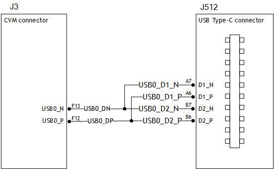
• USB3.1 differential signal pairs (TX* and RX*) wire out from J512 and lead to G22 (UPHY_TX1_N), G23 (UPHY_TX1_P), C22 (UPHY_RX1_N), and C23 (UPHY_RX1_P) on the SOM socket through U522, the USB type-C alt mode switch.

Through the schematic, we can that for J513:
• USB2.0 signal pair is wired to UTMI pad 0 (USB2 port 0).
• USB3.1 signal pairs are wired to UPHY lane 1 (USB3.1 port 2 according to UPHY lane mapping).
The External Connector Class (extcon)
External connectors, which may have different types of cables attached (USB, TA, HDMI, Analog A/V, and others), often have device drivers that detect state changes at the port, and separate device drivers that do something according to the state changes.
The External Connector Class (extcon), introduced in 2012, supports the use of a notifier for passing information such as state changes between device drivers.
Generally, port switching between the roles of an OTG port is controlled by the host driver (xHCI) and device driver (xUDC), and can be defined by the state of the ID pin and the VBUS_DETECT pin.
Taking GPIO_M3 as the VBUS_DETECT pin and GPIO_Q0 as the ID pin, for example:
1. Find the corresponding GPIO states on the VBUS_DETECT pin and ID pin.
Generally, the ID pin is designed as internal pull high (logical high). With an A-plug connected the ID pin is pulled to ground (logical low), while with a B-plug connected or no cable connected it remains logical high.
The operation of the VBUS_DETECT pin depends on the device’s design. Consider the schematic in the following diagram, for example:

With a B-plug connected VBUS_DETECT is logical low, because VBUS is provided from an external power supply, and when no cable is connected it is logical high.
Note: | VBUS_DETECT is initially logical high, then logical low because VBUS is provided by the host controller. Therefore, the state of the VBUS_DETECT pin does not matter when the OTG port is operating in host mode. |
2. Create the table of GPIO states and their corresponding output cable states:
GPIO_Q0 (ID) | GPIO_M3 (VBUS_DETECT) | EXTCON_STATE |
|---|---|---|
1 | 1 | 0x0 (EXCON_NONE) |
0 | 0 | 0x2 (EXTCON_USB_HOST) |
0 | 1 | 0x2 (EXTCON_USB_HOST) |
1 | 0 | 0x1 (EXTCON_USB) |
Under the extcon Node (Not Used on the P2822 Carrier Board)
Port switching between the roles of an OTG port is defined by the state of the ID pin and the VBUS_DETECT pin and the settings of the external connector class.
• compatible: Value must be "extcon-gpio-states".
• extcon-gpio,name: Name of the extcon device.
• gpios: List of the GPIOs.
• extcon-gpio,irq-flags: IRQ flags for GPIO.
• extcon-gpio,debounce: Debounce time in milliseconds.
• extcon-gpio,wait-for-gpio-scan: Wait timeout for scanning all GPIOs’ states after a GPIO state change is detected and debounce time has passed.
• extcon-gpio,out-cable-names: Output cable names.
• extcon-gpio,cable-states: GPIO states and their corresponding output cable states. The value is an array of byte values. Each even-numbered byte is a GPIO state, and the following odd-numbered byte is the corresponding output cable state.
• cable-connected-on-boot: Name of the output cable connected on boot, expressed as an index into extcon-gpio,out-cable-names. The first element is index 0, and so on. If not specified, the system assumes that no cable is to be connected. This property is valid if no GPIOs are provided for cable states.
• wakeup-source: A Boolean; true if the device can wake up the system.
For the detailed information about extcon, refer to the documentation at:
kernel/kernel-4.9/Documentation/devicetree/bindings/extcon/extcon-gpio-states.txt
Note: | OTG port switching between the host driver (xHCI) and device driver (xUDC) roles are controlled by the Cypress Type-C controller. Therefore, this section is not a part of the device-tree for the Jetson AGX Xavier Developer Kit. |
• Create an extcon device node and property list based on the device tree structure described above and the table of GPIO states and corresponding output cable states for GPIO_Q0 and GPIO_M3:
vbus_id_extcon: extcon@1 {
compatible = "extcon-gpio-states";
extcon-gpio,name = "VBUS_ID";
extcon-gpio,wait-for-gpio-scan = <0>;
extcon-gpio,cable-states = <0x3 0x0
0x0 0x2
0x1 0x2
0x2 0x1>;
gpios = <&tegra_main_gpio TEGRA194_MAIN_GPIO(M, 3) 0
&tegra_main_gpio TEGRA194_MAIN_GPIO(Q, 0) 0>;
extcon-gpio,out-cable-names =
<EXTCON_USB EXTCON_USB_HOST EXTCON_NONE>;
#extcon-cells = <1>;
};
For the example of extcon, refer to the device tree's source code at:
hardware/nvidia/platform/t19x/galen/kernel-dts/common/tegra194-e3366-1199-a00.dtsi"
Note: | Check the pinmux table for the GPIO that corresponds to the ID pin and VBUS_DETECT pin. |
Under the ucsi_ccg Node
In the Jetson AGX Xavier Developer Kit role switching of port J512 between host driver (xHCI) and device driver (xUDC) modes is controlled by default by U513, a Cypress Type-C controller, and the ucsi_ccg driver.
typec-extcon
The subnode names must be in the form port-<number>, where <number> is an integer with value 0 or 1 which represents the type-C port (J512/J513).
• #extcon-cells: Number of cells in the extcon specifier. Must be 1.
typec-pd
The name of the subnode must be pd.
• #extcon-cells: Number of cells in the extcon specifier. Must be 1.
For the detailed information about ucsi_ccg, refer to the driver source code at:
kernel/kernel4.9/driver/usb/typec/ucsi/ucsi_ccg.c
Taking J512 USB3.1 type-C connector as an example, create a ucsi_ccg node and property list based on the device tree structure described above for J512:
ucsi_ccg: ucsi_ccg@8 {
status = "okay";
typec-extcon {
typec_port0: port-0 {
status = "okay";
#extcon-cells = <1>;
};
};
typec-pd {
typec_pd: pd {
status = "okay";
#extcon-cells = <1>;
};
};
};
Under the xusb_padctl Node
xusb_padctl settings for an OTG port are the same as for a host-only port except that the mode should be "otg".
Taking J512, the USB3.1 type-C connector, as an example, create a pad/port node and property list:
xusb_padctl: xusb_padctl@3520000 {
...
pads {
usb2 {
lanes {
usb2-0 {
nvidia,function = "xusb";
status = "okay";
};
...
};
};
usb3 {
lanes {
...
usb3-2 {
nvidia,function = "xusb";
status = "okay";
};
...
};
};
};
ports {
usb2-0 {
mode = "otg";
vbus-supply = <&battery_reg>;
status = "okay";
};
...
usb3-2 {
nvidia,usb2-companion = <0>;
status = "okay";
};
...
};
};
Under the xHCI Node
The xHCI settings for an OTG port are the same as for a host-only port except for the addition of extcon settings:
• extcon-cables: OTG support. Must contain a pointer to the excon-cable entry for the USB ID pin. When the extcon cable state is 0, the OTG port transitions to host mode.
Note: | The role of the Jetson AGX Xavier J512 port switch is controlled by U513, a Cypress Type-C controller, and the ucsi_ccg driver. Thus, the extcon-cables entry must be "<entry-of-ucsi_ccg> 1" in the ucsi_ccg node, where 1 is the host mode detect status in ucsi_ccg. |
• extcon-cable-names: Must be "id".
• #extcon-cells: Number of cells in the extcon specifier. Must be 1.
Taking J512, the USB3.1 type-C connector, as an example, create an xHCI node and property list based on the device tree structure described in Under the XHCI Node for a host-only port, plus the extcon settings above:
tegra_xhci: xhci@3610000 {
...
extcon-cables = <&typec_port0 1>;
extcon-cable-names = "id";
#extcon-cells = <1>;
phys = <&{/xusb_padctl@3520000/pads/usb2/lanes/usb2-0}>,
<&{/xusb_padctl@3520000/pads/usb3/lanes/usb3-2}>;
phy-names = "usb2-0", "usb3-2";
nvidia,xusb-padctl = <&xusb_padctl>;
status = "okay";
...
};
Under the xUDC Node
The Jetson AGX Xavier xUDC controller supports both USB 2.0 HighSpeed/FullSpeed and USB 3.1 SuperSpeed protocols.
• extcon-cables: OTG support. Must contains an excon-cable entry which detects USB VBUS pin. When the extcon cable state is 1, OTG port will transition to device mode.
Note: | The role of Jetson AGX Xavier J512 port switch is controlled by U513 Cypress Type-C controller and the ucsi_ccg driver. Hence, the extcon cable entry should be “<entry-of-ucsi_ccg> <host mode detect status in ucsi_ccg>” in ucsi_ccg node, where the <host mode detect status in ucsi_ccg> should be 0. |
• extcon-cable-names: Must be "vbus".
• charger-detector: USB charger detection support. Must be the phandle of the USB charger detection driver DT node.
• phys: An array; must contain a pointer to the node that defines each PHY in phy-names.
• phy-names: An array; must contain an entry for each PHY used by the controller. Names must be in the form <type>-<port_number>, where <type> is one of "usb2" or "usb3".
• nvidia,boost_cpu_freq: The value to which CPU frequency is to be boosted. This is only the minimum frequency; DVFS can scale up CPU frequency further based on need and CPU load. CPU boost frequency through PMQOS is enabled for the xUDC controller only when this field’s value is greater than zero. The boost is applicable only to large bulk transfers on bulk endpoints; other endpoints do not need to be boosted.
• nvidia,xusb-padctl: Must be a pointer to the xusb-padctl node.
For the detailed information about xUDC, refer to the documentation at:
kernel/kernel-4.9
/Documentation/devicetree/bindings/usb/nvidia,tegra-xudc.txt
Taking J512, the USB3.1 type-C connector, as an example, create an xUDC node and property list for J512 based on the device tree structure described above:
tegra_xudc: xudc@3550000 {
extcon-cables = <&typec_port0 0>;
extcon-cable-names = "vbus";
#extcon-cells = <1>;
phys = <&{/xusb_padctl@3520000/pads/usb2/lanes/usb2-0}>,
<&{/xusb_padctl@3520000/pads/usb3/lanes/usb3-2}>;
phy-names = "usb2", "usb3";
nvidia,xusb-padctl = <&xusb_padctl>;
nvidia,boost_cpu_freq = <1200>;
status = "okay";
};
Note: | Before designing your custom board, verify the lane mapping by consulting Jetson AGX Xavier OEM Product Design Guide. |
Flashing the Build Image
When flashing the build image, use your specific board name. The flashing script uses the configuration in the <board>.conf file during the flashing process.
Setting Optional Environment Variables
flash.sh script updates the following environment variables based on board EEPROM and other parameters passed. If you want to give specific values to these variables, define them in the board-specific file board.conf to override the default values.
# Optional Environment Variables:
# BCTFILE ---------------- Boot control table configuration file to be used.
# BOARDID ---------------- Pass boardid to override EEPROM value
# BOARDREV --------------- Pass board_revision to override EEPROM value
# BOARDSKU --------------- Pass board_sku to override EEPROM value
# BOOTLOADER ------------- Bootloader binary to be flashed
# BOOTPARTLIMIT ---------- GPT data limit. (== Max BCT size + PPT size)
# BOOTPARTSIZE ----------- Total eMMC HW boot partition size.
# CFGFILE ---------------- Partition table configuration file to be used.
# CMDLINE ---------------- Target cmdline. See help for more information.
# DEVSECTSIZE ------------ Device Sector size. (default = 512Byte).
# DTBFILE ---------------- Device Tree file to be used.
# EMMCSIZE --------------- Size of target device eMMC (boot0+boot1+user).
# FLASHAPP --------------- Flash application running in host machine.
# FLASHER ---------------- Flash server running in target machine.
# INITRD ----------------- Initrd image file to be flashed.
# KERNEL_IMAGE ----------- Linux kernel zImage file to be flashed.
# MTS -------------------- MTS file name such as mts_si.
# MTSPREBOOT ------------- MTS preboot file name such as mts_preboot_si.
# NFSARGS ---------------- Static Network assignments.
# <C-ipa>:<S-ipa>:<G-ipa>:<netmask>
# NFSROOT ---------------- NFSROOT i.e. <my IP addr>:/exported/rootfs_dir.
# ODMDATA ---------------- Odmdata to be used.
# PKCKEY ----------------- RSA key file to use to sign bootloader images.
# ROOTFSSIZE ------------- Linux RootFS size (internal emmc/nand only).
# ROOTFS_DIR ------------- Linux RootFS directory name.
# SBKKEY ----------------- SBK key file to use to encrypt bootloader images.
# SCEFILE ---------------- SCE firmware file such as camera-rtcpu-sce.img.
# SPEFILE ---------------- SPE firmware file path such as bootloader/spe.bin.
# FAB -------------------- Target board's FAB ID.
# TEGRABOOT -------------- lowerlayer bootloader such as nvtboot.bin.
# WB0BOOT ---------------- Warmboot code such as nvtbootwb0.bin
Note: | All the parameters must be added below the reference to the <xxx>.conf.common file to be reflected in the flashed image. |
Here is an example of environment variable settings:
source "${LDK_DIR}/p2972-0000.conf.common";
PINMUX_CONFIG="tegra19x-mb1-pinmux-p2888-0000-a04-p2822-0000-b01.cfg";
BPFDTB_FILE=tegra194-a02-bpmp-p2888-as-galen-8gb.dtb;
DTB_FILE=tegra194-p2888-0006-p2822-0000.dtb;
TBCDTB_FILE=tegra194-p2888-0006-p2822-0000.dtb;
EMMC_BCT="tegra194-mb1-bct-memcfg-p2888-0006.cfg";
MISC_COLD_BOOT_CONFIG="tegra194-mb1-bct-misc-l4t-p2888-0006.cfg";
To flash the build image
• Execute the following command:
$ sudo ./flash.sh <board> mmcblk0p1