Advanced Learning
This section will focus on the primary Nsight Graphics tools key concepts, advanced information and howto’s.
Introduction
Since the dawn of graphics acceleration, NVIDIA has led the way in creating the most performant and feature-rich GPUs in the world. With each generation, GPUs get faster, and because of that, more complex. To create applications that fully take advantage of the complex capabilities that exist in modern GPUs, you, the programmer, must have a deep understanding of how the GPU operates, as well as a way to see the GPU’s state as it relates to that operation. Fortunately, NVIDIA Graphics Developer Tools have a simple mission: to provide an ecosystem of tools that gives you that power.
This reference guide was created by experts on the Developer Tools team and is meant as a gentle introduction to some critical tools features that will help you debug, profile and ultimately, optimize your application.
Feel free to skip ahead to whichever section is most relevant to you. If you find any information lacking, please contact us at NsightGraphics@nvidia.com so we can make this reference better. In addition to this guide, we’re happy to work with individual developers on training. Lastly, if anything ever goes wrong, remember to use that Feedback Button at the top-right of the tool window so that we have a chance to make the tool work better for you.
GPU Trace
What is it?
GPU Trace is a D3D12/DXR and Vulkan/VKRay graphics profiler used to identify performance limiters in graphics applications. It uses a technique called periodic sampling to gather metrics and detailed timing statistics associated with different GPU hardware units. With Multi-Pass Metrics, the tool can use multiple passes and statistical sampling to collect metrics. For standard metric collection, it takes advantage of specialized Turing hardware to capture this data in a single pass with minimal overhead.
GPU Trace saves this data to a report file and includes “diffing” functionality via a feature called “TraceCompare”. The data is presented as an intuitive visualization on a timeline which is configurable and easy to navigate. The data is organized in a hierarchical top-down fashion so you can observe whole-frame behavior before zooming into individual problem areas. Problems that previously required guessing & testing can now be visually identified at a glance.
In this section we will focus on the key-concepts the GPU Trace tool introduces and in depth explanation of the data it retrieves.
To learn how to use the tools go to the activities section in the user guide: here.
To understand the UI components GPU Trace UI section in the User Interface Reference here.
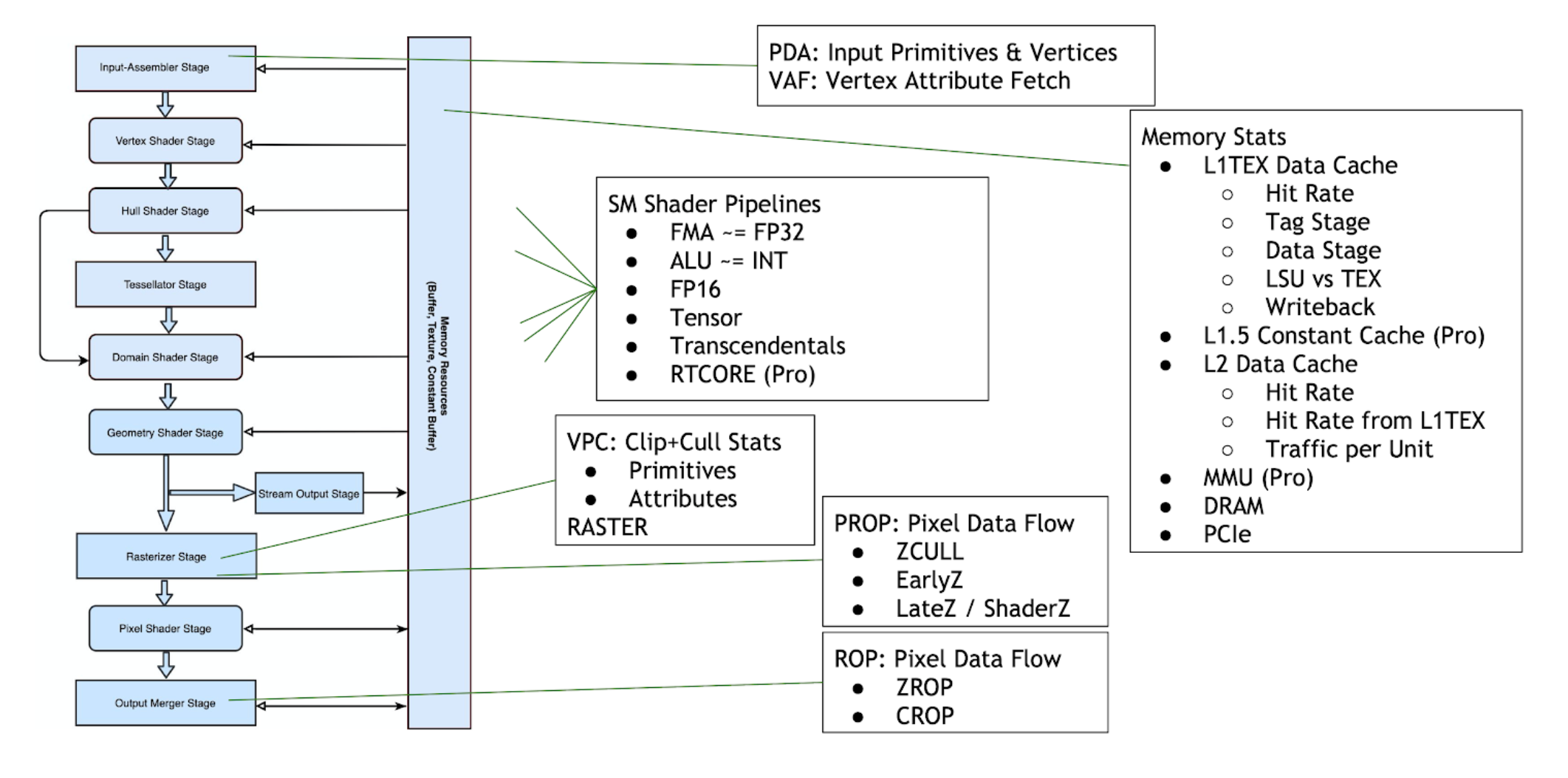
Overview of the GPU
GPU Trace allows you to observe metrics across all stages of the D3D12 and Vulkan graphics pipeline. The following diagram names the NVIDIA hardware units related to each logical pipeline state:
Units Throughput
The Unit Throughputs row overlays the %-of-max-throughput of every hardware unit in the GPU. Multiple units can concurrently reach close to 100% at any moment in time.
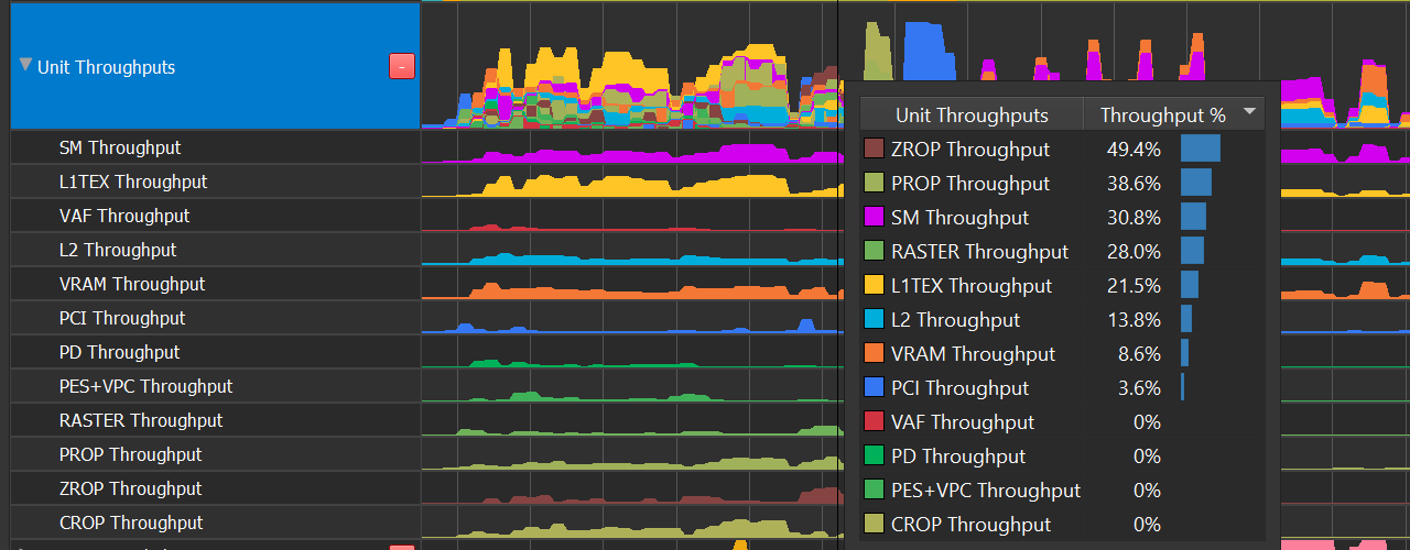
Unit |
Pipeline Area |
Description |
|---|---|---|
SM |
Shader |
The Streaming Multiprocessor executes shader code. |
L1TEX |
Memory |
The L1TEX unit contains the L1 data cache for the SM, and two parallel pipelines: the LSU or load/store unit, and TEX for texture lookups and filtering. |
L2 |
Memory |
The L2 cache serves all units on the GPU, and is a central point of coherency. |
VRAM |
Memory |
|
PD |
World Pipe |
The Primitive Distributor fetches indices from the index buffer, and sends triangles to the vertex shader. |
VAF |
World Pipe |
The Vertex Attribute Fetch unit reads attribute values from memory and sends them to the vertex shader. VAF is part of the Primitive Engine. |
PES+VPC |
World Pipe |
The Primitive Engine orchestrates the flow of primitive and attribute data across all world pipe shader stages (Vertex, Tessellation, Geometry). PES contains the stream (transform feedback) unit. The VPC unit performs clip and cull. |
RASTER |
Screen Pipe |
The Raster units receives primitives from the world pipe, and outputs pixels (fragments) and samples (coverage masks) for the PROP, Pixel Shader, and ROP to process. |
PROP |
Screen Pipe |
The Pre-ROP unit orchestrates the flow of depth and color pixels (fragments) and samples, for final output. PROP enforces the API ordering of pixel shading, depth testing, and color blending. Early-Z and Late-Z modes are handled in PROP. |
ZROP |
Screen Pipe |
The Depth Raster Operation unit performs depth tests, stencil tests, and depth/stencil buffer updates. |
CROP |
Screen Pipe |
The Color Raster Operation unit performs the final color blend and render-target updates. CROP implements the “advanced blend equation” |
SM Occupancy Rows
The SM Occupancy row shows warp slot residency over time. Each Turing SM has 32 warp slots, where launched warps reside while they take turns issuing instructions.
Asynchronous Compute
The only way to concurrently run compute and 3D is by simultaneously:
sending 3D work to the DIRECT queue
sending compute work to an ASYNC_COMPUTE queue
On Ampere, you can also dispatch concurrent compute workloads by dispatching it on both the DIRECT and ASYNC_COMPUTE queue.
You can detect whether a program is taking advantage of async compute in several ways:
The “Compute In Flight” row contains an “Async Compute In Flight” counter.
Observe when the compute warps executed on the SM Occupancy row, and determine if they were Sync or Async based on the color of the “Compute In Flight” row.
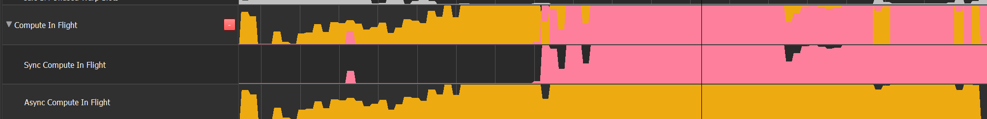
Look for multiple queue rows; the ASYNC_COMPUTE queue will appear as something other than Q0.
Compute will only run simultaneously with graphics if submitted on from an ASYNC_COMPUTE queue. This can disambiguate the SM Occupancy row.

Warp Can’t Launch Reasons
When a draw call or compute dispatch enqueues more work than can fit onto the SMs all-at-once, the SMs will report that “additional warps can’t launch.” We can graph these signals over time to determine the limiting factor.
3D Shaders
3D warps may not launch due to the following reasons:
Register Allocation
Warp Allocation
Attribute Allocation (ISBEs for VTG, or TRAM for PS)
GPU Trace allows you to determine the following:
When Pixel Shaders can’t launch, for any reason.
When Pixel Shaders launch was register limited.
The warp-allocation limited regions in the Warp Occupancy chart. There are no free slots when there are no gray regions.
By deduction, if SM Occupancy shows a large region of pixel warps with no limiter visible, it either means:
There was no warp launch stall, but rather very long running warps [unlikely], OR
Warp launch was stalled due to attribute allocation.
Compute Shaders Compute warps may not launch due to the following reasons:
Register Allocation
Warp Allocation
CTA Allocation
Shared Memory Allocation
GPU Trace allow you to determine the following:
When Compute Shaders should be running in the Compute In Flight row.
When Compute Shader launch was register limited.
The warp-allocation limited regions in the Warp Occupancy chart. There are no free slots when there are no gray regions.
By deduction, if SM Occupancy shows a large region of compute warps with no limiter visible, it eithers means:
There was no warp launch stall, but rather very long running warps [unlikely], OR
One of the other reasons (CTAs, Shared Memory) was the reason.
Further disambiguating between 4a and 4b above:
Are the CTA dimensions (HLSL numthreads) the theoretical occupancy limiter for your shader? A thread group with 32 threads or fewer will be limited to half occupancy. Increasing to 64 threads per CTA will relieve this issue.
Is the shared memory size per CTA the theoretical occupancy limiter for your shader? (HLSL groupshared variables) Does (numCTAs * shmemSizePerCTA) exceed the per-SM limit of 64KiB [compute-only mode] or 32KiB [SCG mode]?
SM Throughput
SM Throughput reveals the most common computational pipeline limiters in shader code:
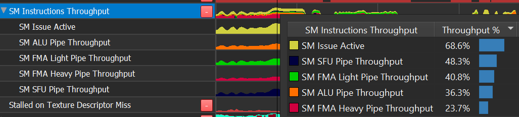
Issue Active : instruction-issue limited
ALU Pipe : INT other than multiply, bit manipulation, lower frequency FP32 like comparison and min/max.
FMA Pipe : FP32 add and multiply, integer multiply.
FP16+Tensor : FP16 instructions which execute a vec2 per instruction, and Tensor ops used by deep learning.
SFU Pipe : transcendentals (sqrt, rsqrt, sin, cos, log, exp, …)
Pipes not covered in the SM Throughput: IPA, LSU, TEX, CBU, ADU, RTCORE, UNIFORM.
LSU and TEX are never limiters in the SM; see L1 Throughput instead.
IPA traffic to TRAM is counted as part of LSU
RTCORE has its own Throughput metric
UNIFORM and CBU are unaccounted for, but rarely a limiter
Problem Solving:
If FP32 is high, consider using FP16 instead.
In theory, a 2X speedup is possible due solely to pipeline width.
In theory, a 3X speedup is possible by perfectly balancing FP32 and FP16.
L1 Throughput
GPU Trace exposes a simplified model of the L1TEX Data Cache, that still reveals the most common types of memory limiters in shader programs.
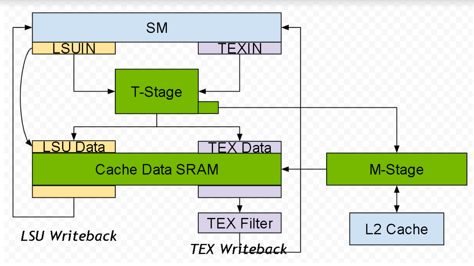
The Turing and GA10x L1TEX Caches share a similar design, capable of concurrent accesses:
Input: Simultaneously accepting an LSU instruction and TEX quad per cycle
Input: LSUIN accepts 16 threads’ addresses per cycle from AGU
Data: Simultaneously reading or writing the Data SRAM for LSU and TEX.
Writeback: Simultaneously returning data for LSU and TEX reads
Additional cache properties:
The T-Stage (cache tags), Data-Stage, and M-Stage are shared between LSU and TEX
The T-Stage address coalescer can output up to 4 tags per cycle, for divergent accesses. This ensures T-Stage is almost never a limiter, compared to Data-Stage
Per cycle, M-Stage can simultaneously read from L2 and write to L2. There is a crossbar (XBAR) between M-Stage and L2, not pictured above
In this simplified model, memory and texture requests follow these paths:
Local/Global Instruction → LSUIN → T-Stage → LSU Data → LSU Writeback → SM
Shared Memory Instruction → LSUIN → LSU Data → LSU Writeback → RF
Includes compute shared memory and 3D shader attributes
A few non-memory ops like HLSL Wave Broadcast are counted here
Texture/Surface Read → TEXIN → T-Stage → TEX Data → Filter → Writeback → SM
Includes texture fetches, texture loads, surface loads, and surface atomics
Surface Write → TEXIN… → T-Stage → LSU Data → Writeback → RF
Surface writes cross over to the LSU Data path
Memory Barriers → LSUIN & TEXIN → … flows through both sides of the pipe
Primitive Engine attribute writes to (ISBE, TRAM) → LSU Data
Primitive Engine attribute reads from ISBE → LSU Data
Local/Global/Texture/Surface→ T-Stage [miss!] → M-Stage → XBAR → L2 → XBAR → M-Stage → Cache Data SRAM
Turing Problem Solving
Turing reports the following activity:
Throughput of LSU Data and TEX Data
Separate counters in LSU Data for Local/Global vs. Shared memory
Throughput of LSU Writeback, and TEX Filter
By comparing the values of the available throughputs, we can draw the following conclusions:
All values are equal : most likely request limited
TEX Data > others : bandwidth limited; cachelines/instruction > 1
TEX Filter > others : expensive filtering (Trilinear/Aniso) OR Texture writeback limited due to a wide sampler format (or surface format when sampler disabled)
LSU Data > others : the possibilities are:
Pure bandwidth limited
Cachelines per instruction > 1, causing serialization
Shared memory bank conflicts, causing serialization
Vectored shared memory accesses (64-bit, 128-bit) requiring multi-cycle access
Heavy use of SHFL (HLSL Wave Broadcast)
LSU Writeback > others : limited by coalesced wide loads (64-bit or 128-bit)
Note: this implies efficient use of LSU Data
LSU LG Data or TEX Data close to 100% : implies a high hit-rate
If Sector Hit Rate is low : may imply latency-bound by L2 or VRAM accesses
GA10x Problem Solving
GA10x reports the following activity:
Throughput of LSU Data and TEX Data
Separate counters in LSU Data per Local/Global, Surface, and Shared memories
Throughput of LSU Writeback, TEX Filter, and TEX Writeback
L1TEX Sector Hit-Rate - Reports the collective hit-rate for Local, Global, Texture, Surface - Note that shared memory and 3D attributes do not contribute to the hit-rate
By comparing the values of the available throughputs, we can draw the following conclusions:
All values are equal : most likely request limited
TEX Data > others : bandwidth limited; cachelines/instruction > 1
TEX Filter > others : expensive filtering (Trilinear/Aniso)
TEX Writeback > others : limited wide sampler format (or surface format when sampler disabled)
LSU Data > others : the possibilities are:
Pure bandwidth limited
Cachelines per instruction > 1, causing serialization
Shared memory bank conflicts, causing serialization
Vectored shared memory accesses (64-bit, 128-bit) requiring multi-cycle access
Heavy use of HLSL Wave Broadcast
LSU Writeback > others : limited by coalesced wide loads (64-bit or 128-bit)
Note: this implies efficient use of LSU Data
LSU LG Data or TEX Data close to 100% : implies a high hit-rate; cross-check against the L1TEX Sector Hit Rate
If Sector Hit Rate is low : may imply being latency-bound by L2 or VRAM accesses
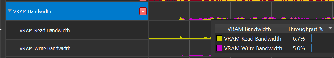
VRAM
The GPU’s VRAM is built with DRAM. DRAM is a half duplex interface, meaning the same wires are used for read and write, but not simultaneously. This is why the total VRAM bandwidth is the sum of read and write.
The VRAM Bandwidth row shows bandwidth as a stacked graph, making it easy to visualize the balance between read and write traffic. VRAM traffic implies either L2 cache misses, or L2 writeback. In either case, high VRAM traffic can be a symptom of poor L2 cache usage — either too large a working set, or sub-optimal access patterns.
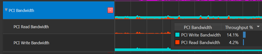
PCI Bandwidth
The GPU connects to the rest of the computer via PCI Express (PCIe). PCIe is a full duplex interface, meaning separate wires are used for reads and writes, and these can occur simultaneously. This is why the PCIe row is displayed as an overlay, where reads and writes can independently reach 100%.
When the GR engine is idle (neither graphics nor compute running), it is often due to a data dependency, where a previous data transfer (DMA copy) must complete before draws or compute dispatches can start. Compare the GPU Active row against the Throughputs row to confirm that hypothesis.