Pinouts Description
The below table lists the NC-SI pins description. For further details, please refer to NC-SI Management Interface.
Pin# | Signal Name | I/O | Description |
1 | REF_CLK | I | 50M REF CLK for NCSI BUS |
2 | GND | GND | Ground |
3 | ARB_IN | I | NCSI hardware arbitration input |
4 | GND | GND | Ground |
5 | ARB_OUT | O | NCSI hardware arbitration output |
6 | GND | GND | Ground |
7 | RX_D0 | O | Receive data |
8 | GND | GND | Ground |
9 | RX_D1 | O | Receive data |
10 | GND | GND | Ground |
11 | CRS_DV | O | Carrier sense/Receive Data Valid |
12 | GND | GND | Ground |
13 | TX_D0 | I | Transmit data |
14 | RSRV | Reserved | |
15 | TX_D1 | I | Transmit data |
16 | GND | GND | Ground |
17 | TX_EN | I | Transmit enable |
18 | GND | GND | Ground |
19 | NC | ||
20 | GND | GND | Ground |
21 | I2C_SDA | B | I2C Serial Data |
22 | GND | GND | Ground |
23 | I2C_SCL | I | I2C Serial Clock |
24 | GND | GND | Ground |
25 | GND | GND | Ground |
26 | GND | GND | Ground |
27 | 3.3V | VDD | Power |
28 | 3.3V | VDD | Power |
29 | 3.3V | VDD | Power |
30 | 3.3V | VDD | Power |
The below table provides the External Power Supply pins of the external power supply interfaces on the multi-host motherboard. For further details, please refer to External PCIe Power Supply Connector.
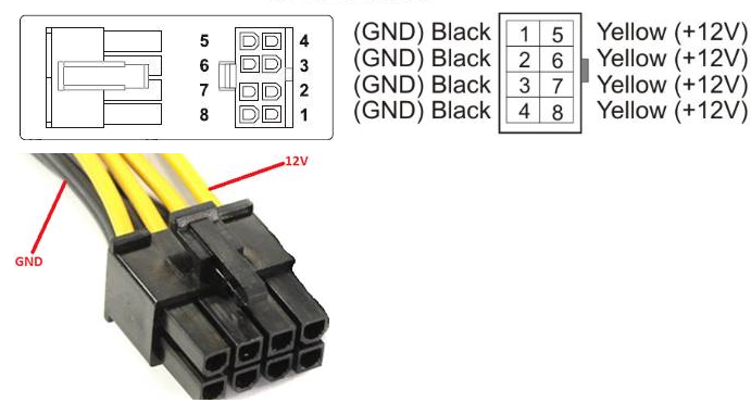
The mechanical pinout of the 8-pin external +12V power connector is shown below. The +12V connector is a GPU power PCIe standard connector. Care should be taken to ensure the power is applied to the correct pins as some 8-pin ATX type connector can have different pinouts.
Pin# | Signal Name | Description |
1 | GND | Power Return |
2 | GND | Power Return |
3 | GND | Power Return |
4 | GND | Power Return |
5 | 12V | ATX Supplied 12V |
6 | 12V | ATX Supplied 12V |
7 | 12V | ATX Supplied 12V |
8 | 12V | ATX Supplied 12V |