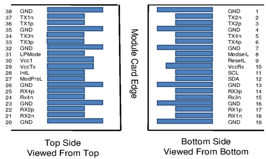
Pin Description
The Direct Attach Copper (DAC) pin assignment is SFF-8679 compliant.
Pin | Symbol | Description | Pin | Symbol | Description |
1 | GND | Ground | 20 | GND | Ground |
2 | Tx2n | Transmitter Inverted Data Input | 21 | Rx2n | Receiver Inverted Data Output |
3 | Tx2p | Transmitter Non-Inverted Data Input | 22 | Rx2p | Receiver Non-Inverted Data Output |
4 | GND | Ground | 23 | GND | Grounds |
5 | Tx4n | Transmitter Inverted Data Input | 24 | Rx4n | Receiver Inverted Data Output |
6 | Tx4p | Transmitter Non-Inverted Data Input | 25 | Rx4p | Receiver Non-Inverted Data Output |
7 | GND | Ground | 26 | GND | Ground |
8 | ModSelL | Module Select | 27 | ModPrsL | Module Present |
9 | ResetL | Module Reset | 28 | IntL | Interrupt |
10 | Vcc Rx | +3.3V Power Supply Receiver | 29 | Vcc Tx | +3.3V Power Supply Transmitter |
11 | SCL | 2-wire Serial Interface Clock | 30 | Vcc1 | +3.3V Power Supply |
12 | SDA | 2-wire Serial Interface Data | 31 | LPMode | Low Power Mode |
13 | GND | GND | 32 | GND | Ground |
14 | Rx3p | Receiver Non-Inverted Data Output | 33 | Tx3p | Transmitter Non-Inverted Data Input |
15 | Rx3n | Receiver Inverted Data Output | 34 | Tx3n | Transmitter Inverted Data Input |
16 | GND | Ground | 35 | GND | Ground |
17 | Rx1p | Receiver Non-Inverted Data Output | 36 | Tx1p | Transmitter Non-Inverted Data Input |
18 | Rx1n | Receiver Inverted Data Output | 37 | Tx1n | Transmitter Inverted Data Input |
19 | GND | Ground | 38 | GND | Ground |
QSFP56 Module Pad Layout