Pin Descriptions
The device is compliant with the Specification for OSFP (Octal Small Form Factor Pluggable) Modules, Rev. 1.12, see www.osfpmsa.org.
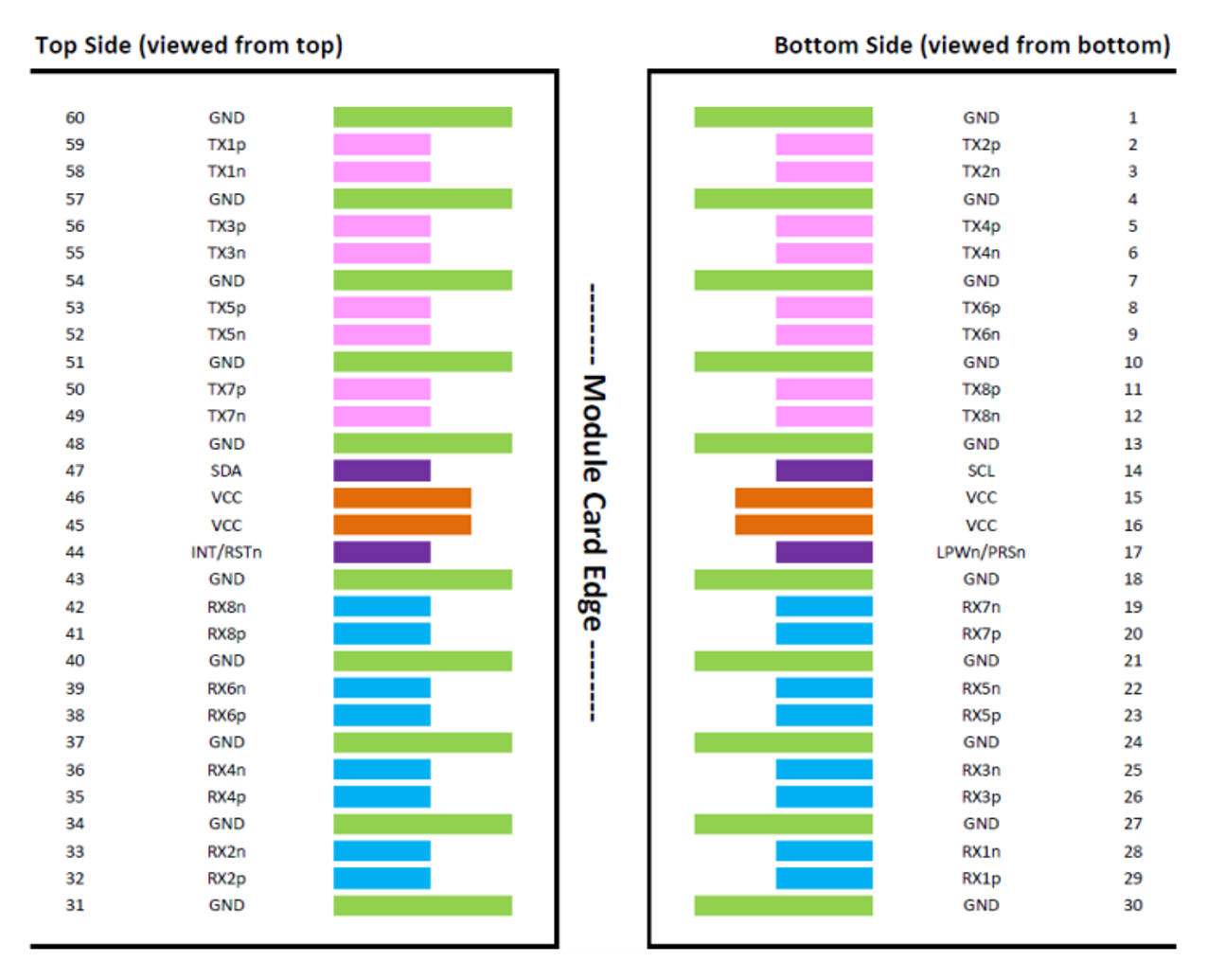
The pin assignment for the electrical (host) interface is shown below.
Pin | Symbol | Description | Pin | Symbol | Description |
1 | GND | Ground | 31 | GND | Ground |
2 | Tx2p | Transmitter Non-Inverted Data Input | 32 | Rx2p | Receiver Non-Inverted Data Output |
3 | Tx2n | Transmitter Inverted Data Input | 33 | Rx2n | Receiver Inverted Data Output |
4 | GND | Ground | 34 | GND | Grounds |
5 | Tx4p | Transmitter Non-Inverted Data Input | 35 | Rx4p | Receiver Non-Inverted Data Output |
6 | Tx4n | Transmitter Inverted Data Input | 36 | Rx4n | Receiver Inverted Data Output |
7 | GND | Ground | 37 | GND | Ground |
8 | Tx6p | Transmitter Non-Inverted Data Input | 38 | Rx6p | Receiver Non-Inverted Data Output |
9 | Tx6n | Transmitter Inverted Data Input | 39 | Rx6n | Receiver Inverted Data Output |
10 | GND | Ground | 40 | GND | Ground |
11 | Tx8p | Transmitter Non-Inverted Data Input | 41 | Rx8p | Receiver Non-Inverted Data Output |
12 | Tx8n | Transmitter Inverted Data Input | 42 | Rx8n | Receiver Inverted Data Output |
13 | GND | Ground | 43 | GND | Ground |
14 | SCL | 2-wire serial interface clock | 44 | INT / RSTn | Module Interrupt / Module Reset |
15 | VCC | +3.3V Power | 45 | VCC | +3.3V Power |
16 | VCC | +3.3V Power | 46 | VCC | +3.3V Power |
17 | LPWn / PRSn | Low-Power Mode / Module Present | 47 | SDA | 2-wire Serial interface data |
18 | GND | Ground | 48 | GND | Ground |
19 | Rx7n | Receiver Inverted Data Output | 49 | Tx7n | Transmitter Inverted Data Input |
20 | Rx7p | Receiver Non-Inverted Data Output | 50 | Tx7p | Transmitter Non-Inverted Data Input |
21 | GND | Ground | 51 | GND | Ground |
22 | Rx5n | Receiver Inverted Data Output | 52 | Tx5n | Transmitter Inverted Data Input |
23 | Rx5p | Receiver Non-Inverted Data Output | 53 | Tx5p | Transmitter Non-Inverted Data Input |
24 | GND | Ground | 54 | GND | Ground |
25 | Rx3n | Receiver Inverted Data Output | 55 | Tx3n | Transmitter Inverted Data Input |
26 | Rx3p | Receiver Non-Inverted Data Output | 56 | Tx3p | Transmitter Non-Inverted Data Input |
27 | GND | Ground | 57 | GND | Ground |
28 | Rx1n | Receiver Inverted Data Output | 58 | Tx1n | Transmitter Inverted Data Input |
29 | Rx1p | Receiver Non-Inverted Data Output | 59 | Tx1p | Transmitter Non-Inverted Data Input |
30 | GND | Ground | 60 | GND | Ground |
OSFP Module Pad Layout