Pin Descriptions
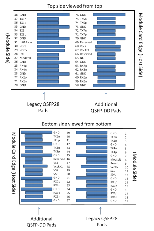
The head end of the MCP7F80 cable has the pad assignment shown below, which is compliant with the QSFP-DD Hardware Specification [2].
|
Pin |
Symbol |
Description |
Pin |
Symbol |
Description |
|
1 |
GND |
Ground |
39 |
GND |
Ground |
|
2 |
Tx2n |
Transmitter Inverted Data Input |
40 |
Tx6n |
Transmitter Inverted Data Input |
|
3 |
Tx2p |
Transmitter Non-Inverted Data Input |
41 |
Tx6p |
Transmitter Non-Inverted Data Input |
|
4 |
GND |
Ground |
42 |
GND |
Ground |
|
5 |
Tx4n |
Transmitter Inverted Data Input |
43 |
Tx8n |
Transmitter Inverted Data Input |
|
6 |
Tx4p |
Transmitter Non-Inverted Data Input |
44 |
Tx8p |
Transmitter Non-Inverted Data Input |
|
7 |
GND |
Ground |
45 |
GND |
Ground |
|
8 |
ModSelL |
Module Select |
46 |
Reserved |
|
|
9 |
ResetL |
Module Reset |
47 |
VS1 |
Module Vendor Specific 1 |
|
10 |
VccRx |
+3.3V Power Supply Receiver |
48 |
VccRx1 |
+3.3V Power Supply Receiver |
|
11 |
SCL |
2-wire Serial Interface Clock |
49 |
VS2 |
Module Vendor Specific 2 |
|
12 |
SDA |
2-wire Serial Interface Data |
50 |
VS3 |
Module Vendor Specific 3 |
|
13 |
GND |
GND |
51 |
GND |
Ground |
|
14 |
Rx3p |
Receiver Non-Inverted Data Output |
52 |
Rx7p |
Receiver Non-Inverted Data Output |
|
15 |
Rx3n |
Receiver Inverted Data Output |
53 |
Rx7n |
Receiver Inverted Data Output |
|
16 |
GND |
Ground |
54 |
GND |
Ground |
|
17 |
Rx1p |
Receiver Non-Inverted Data Output |
55 |
Rx5p |
Receiver Non-Inverted Data Output |
|
18 |
Rx1n |
Receiver Inverted Data Output |
56 |
Rx5n |
Receiver Inverted Data Output |
|
19 |
GND |
Ground |
57 |
GND |
Ground |
|
20 |
GND |
Ground |
58 |
GND |
Ground |
|
21 |
Rx2n |
Receiver Inverted Data Output |
59 |
Rx6n |
Receiver Inverted Data Output |
|
22 |
Rx2p |
Receiver Non-Inverted Data Output |
60 |
Rx6p |
Receiver Non-Inverted Data Output |
|
23 |
GND |
Ground |
61 |
GND |
Grounds |
|
24 |
Rx4n |
Receiver Inverted Data Output |
62 |
Rx8n |
Receiver Inverted Data Output |
|
25 |
Rx4p |
Receiver Non-Inverted Data Output |
63 |
Rx8p |
Receiver Non-Inverted Data Output |
|
26 |
GND |
Ground |
64 |
GND |
Ground |
|
27 |
ModPrsL |
Module Present |
65 |
NC |
|
|
28 |
IntL |
Interrupt |
66 |
Reserved |
|
|
29 |
VccTx |
+3.3V Power Supply Transmitter |
67 |
VccTx1 |
+3.3V Power Supply Transmitter |
|
30 |
Vcc1 |
+3.3V Power Supply |
68 |
Vcc2 |
+3.3V Power Supply |
|
31 |
LPMode |
Low Power Mode |
69 |
Reserved |
|
|
32 |
GND |
Ground |
70 |
GND |
Ground |
|
33 |
Tx3p |
Transmitter Non-Inverted Data Input |
71 |
Tx7p |
Transmitter Non-Inverted Data Input |
|
34 |
Tx3n |
Transmitter Inverted Data Input |
72 |
Tx7n |
Transmitter Inverted Data Input |
|
35 |
GND |
Ground |
73 |
GND |
Ground |
|
36 |
Tx1p |
Transmitter Non-Inverted Data Input |
74 |
Tx5p |
Transmitter Non-Inverted Data Input |
|
37 |
Tx1n |
Transmitter Inverted Data Input |
75 |
Tx5n |
Transmitter Inverted Data Input |
|
38 |
GND |
Ground |
76 |
GND |
Ground |
QSFP-DD Module Pad Layout
The 50G ‘tails’ of the MCP7F80 cable are compliant with the SFF-8431 specifications. The connectors have the pin assignment shown below.
|
Pin |
Symbol |
Description |
|
1 |
VeeT |
Module Transmitter Ground |
|
2 |
Tx_Fault |
Module Transmitter Fault. Connected to GND. |
|
3 |
Tx_Disable |
Not used. Connected to 3.3V |
|
4 |
SDA |
2-wire Serial Interface Data Line |
|
5 |
SCL |
2-wire Serial Interface Clock |
|
6 |
Mod_ABS |
Module Absent. Grounded within the module |
|
7 |
RS0 |
Rate Select 0, optionally controls SFP+ module receiver. Pulled down to GND. Not used. |
|
8 |
Rx_LOS |
Not used. Connected to GND. |
|
9 |
RS1 |
Rate Select 1, optionally controls SFP+ module transmitter. Not used. |
|
10 |
VeeR |
Module Receiver Ground |
|
11 |
VeeR |
Module Receiver Ground |
|
12 |
RD- |
Receiver Inverted Data Output |
|
13 |
RD+ |
Receiver Non-Inverted Data Output |
|
14 |
VeeR |
Module Receiver Ground |
|
15 |
VccR |
Module Receiver Power Supply |
|
16 |
VccT |
Module Transmitter Power Supply. Connected to 3.3V. |
|
17 |
VeeT |
Module Transmitter Ground |
|
18 |
TD+ |
Transmitter Non-Inverted Data Input. AC coupled |
|
19 |
TD- |
Transmitter Inverted Data Input. AC coupled |
|
20 |
VeeT |
Module Transmitter Ground |
SFP+ Module Pad Layout