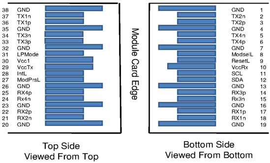
Pin Descriptions
|
Pin # |
Symbol |
Description |
Pin # |
Symbol |
Description |
|
1 |
GND |
Ground |
20 |
GND |
Ground |
|
2 |
Tx2n |
Connected to Port 2 lane Rx |
21 |
Rx2n |
Connected to Port 2 lane Tx |
|
3 |
Tx2p |
Connected to Port 2 lane Rx |
22 |
Rx2p |
Connected to Port 2 lane Tx |
|
4 |
GND |
Ground |
23 |
GND |
Grounds |
|
5 |
Tx4n |
Connected to Port 4 lane Rx |
24 |
Rx4n |
Connected to Port 4 lane Tx |
|
6 |
Tx4p |
Connected to Port 4 lane Rx |
25 |
Rx4p |
Connected to Port 4 lane Tx |
|
7 |
GND |
Ground |
26 |
GND |
Ground |
|
8 |
Mod-SelL |
Cable Select |
27 |
ModPrsL |
Cable Present |
|
9 |
ResetL |
Cable Reset |
28 |
IntL |
Interrupt |
|
10 |
Vcc Rx |
+3.3V Power supply receiver |
29 |
Vcc Tx |
+3.3V Power supply transmitter |
|
11 |
SCL |
2-wire serial interface clock |
30 |
Vcc1 |
+3.3V Power Supply |
|
12 |
SDA |
2-wire serial interface data |
31 |
LPMode |
Low Power Mode |
|
13 |
GND |
GND |
32 |
GND |
Ground |
|
14 |
Rx3p |
Connected to Port 3 lane Tx |
33 |
Tx3p |
Connected to Port 3 lane Rx |
|
15 |
Rx3n |
Connected to Port 3 lane Tx |
34 |
Tx3n |
Connected to Port 3 lane Rx |
|
16 |
GND |
Ground |
35 |
GND |
Ground |
|
17 |
Rx1p |
Connected to Port 1 lane Tx |
36 |
Tx1p |
Connected to Port 1 lane Rx |
|
18 |
Rx1n |
Connected to Port 1 lane Tx |
37 |
Tx1n |
Connected to Port 1 lane Rx |
|
19 |
GND |
Ground |
38 |
GND |
Ground |
QSFP28 Module Pad Layout
The MFA7A50 AOC is SFF-8636 compliant. This means that the control signals shown in the pad layout support the following functions:
|
ModPrsL |
Module Present pin, grounded inside the module. Terminated with pull-up in the host system. Asserted low when the transceiver is inserted, whereby the host detects the presence of the transceiver. |
|
ModSelL |
Module Select input pin, terminated high in the module. Only when held low by the host, the module responds to 2-wire serial communication commands. The ModSelL enables multiple modules to share a single 2-wire interface bus. |
|
ResetL |
Reset input pin, pulled high in the module. A low level on the ResetL pin for longer than the minimum pulse length (t_Reset_init) initiates a complete module reset, returning all user module settings to their default state. During reset the host shall disregard all status bits until the module indicates completion of the reset interrupt by asserting IntL signal low with the Data_Not_Ready bit negated. Note that on power up (including hot insertion) the module completes the reset interrupt without requiring a reset. |
|
LPMode |
Low Power Mode input, pulled up inside the module. The transceiver starts up in low power mode, i.e. <1.5 W with the two-wire interface active. The host system can read the power class declaration from the transceiver and determine if it has enough power to enable the high-speed operation/high power mode of the transceiver. This can be done by asserting LPMode low or by use of the Power_over-ride and Power_set control bits (Address A0h, byte 93 bits 0,1). |
|
IntL |
Interrupt Low is an open-collector output, terminated high in the host system. A “Low” indicates a possible module operational fault or a status critical to the host system, e.g. temperature alarm. The host identifies the source of the interrupt using the 2-wire serial interface. The INTL pin is de-asserted “High” after completion of reset, when byte 2 bit 0 (Data Not Ready) is read with a value of ‘0’. |
The low-speed signals are Low Voltage TTL (LVTTL) compliant (except for SCL and SDA signals).
|
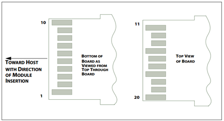
Pin # |
Connector Pin Name |
Port A Signal Name |
|
1 |
VeeT |
Module Transmitter Ground |
|
2 |
Tx_Fault |
Module Transmitter Fault |
|
3 |
Tx_Disable |
Transmitter Disable. Turns off transmitter laser output |
|
4 |
SDA |
2-wire Serial Interface Data Line |
|
5 |
SCL |
2-wire Serial Interface Clock |
|
6 |
Mod_ABS |
Module Absent. Grounded within the module |
|
7 |
RS0 |
Rate Select 0, optionally controls SFP+ module receiver |
|
8 |
Rx_LOS |
Receiver Loss of Signal Indication |
|
9 |
RS1 |
Rate Select 1, optionally controls SFP+ module transmitter |
|
10 |
VeeR |
Module Receiver Ground |
|
11 |
VeeR |
Module Receiver Ground |
|
12 |
RD- |
Receiver Inverted Data Output |
|
13 |
RD+ |
Receiver Non-Inverted Data Output |
|
14 |
VeeR |
Module Receiver Ground |
|
15 |
VccR |
Module Receiver Power Supply |
|
16 |
VccT |
Module Transmitter Power Supply |
|
17 |
VeeT |
Module Transmitter Ground |
|
18 |
TD+ |
Transmitter Non-Inverted Data Input. AC coupled |
|
19 |
TD- |
Transmitter Inverted Data Input. AC coupled |
|
20 |
VeeT |
Module Transmitter Ground |
SFP28 Module Pad Layout
The 100 Gb transceiver complies with the SFF-8665 specification, and the 25 Gb transceivers with the SFF-8402 specification. Both have the following functional and Digital Diagnostic Monitoring (DDM) features:
Physical layer link optimization:
Tx input equalization programmable in 11 levels from 0 to 10 dB
Rx output amplitude programmable in 2 levels up to 400 mVpp
Rx output pre-emphasis programmable in 8 levels from 0 to 7 dB
Selectable Tx/Rx CDR control
Digital Diagnostic Monitoring (DDM) – Data Readout and Warning/Alarm Indication:
Rx receive optical power monitor
Tx transmit optical power monitor
Tx bias current monitor
Supply voltage monitor
Transceiver case temperature monitor
Other SFF-8636 functions and interrupt indications:
Tx & Rx LOS indication
Tx & Rx LOL indication
Tx fault indication
Selectable Tx Squelch per lane
Selectable Tx & Rx disable per lane
The DDM functions comply with the SFF-8636 specifications for the 100 Gb end, and with the SFF-8472 specifications for the 25 Gb end.