Specifications
Absolute maximum ratings are those beyond which damage to the device may occur.
Prolonged operation between the operational specifications and absolute maximum ratings is not intended and may cause permanent device degradation.
|
Parameter |
Symbol |
Min |
Max |
Units |
|
Storage Temperature |
TS |
-40 |
85 |
°C |
|
Operating Case Temperature |
TOP |
0 |
70 |
°C |
|
Supply Voltage |
Vcc |
-0.5 |
3.6 |
V |
|
Relative Humidity (non-condensing) |
RH – Option 1 |
5 |
65 |
% |
|
Control Input Voltage |
VI |
-0.3 |
Vcc+0.5 |
V |
Maximum switch ambient temperature for reverse (front to back) airflow on QM9700 is 40°C with all fans, and 35°C in case of fan failure.
|
Parameter |
Symbol |
Min |
Typ |
Max |
Units |
|
Power Supply Voltage |
VCC |
3.135 |
3.3 |
3.465 |
V |
|
Instantaneous peak current at hot plug |
ICC_IP |
- |
- |
6800 |
mA |
|
Sustained peak current at hot plug |
ICC_SP |
- |
- |
5670 |
mA |
|
Maximum Power Dissipation |
PD |
- |
16 |
17 |
W |
|
Maximum Power Dissipation, Low Power Mode |
PDLP |
- |
- |
1.5 |
W |
|
Signaling Rate per Lane |
SRL |
- |
53.125 |
- |
GBd |
|
Two Wire Serial Interface Clock Rate |
- |
100 |
- |
1000 |
kHz |
|
Power Supply Noise Tolerance (10Hz - 10MHz) |
- |
- |
- |
25 |
mV |
|
Rx Differential Data Output Load |
- |
- |
100 |
- |
Ohm |
|
Operating Distance |
- |
2 |
- |
(OPN dependent) |
m |
|
Parameter |
Symbol |
Min |
Typ |
Max |
Units |
|
Receiver (Module Output) |
|||||
|
Peak-peak AC common-mode voltage |
VCMLF |
17 |
- |
32 |
mV |
|
VCMFB |
- |
- |
80 |
||
|
Differential output Voltage (Long mode) |
- |
- |
900 |
mV |
|
|
Differential output Voltage (Short mode) |
- |
- |
600 |
mV |
|
|
Eye height, differential |
15 |
- |
- |
mV |
|
|
Differential Termination Mismatch |
- |
- |
10 |
% |
|
|
Transition Time (min, 20% to 80%) |
8.5 |
- |
- |
ps |
|
|
DC common mode Voltage |
-350 |
- |
2850 |
mV |
|
|
Transmitter (Module Input) |
|||||
|
Differential pk-pk input Voltage tolerance |
750 |
- |
- |
mV |
|
|
Differential termination mismatch |
- |
- |
10 |
% |
|
|
Single-ended voltage tolerance range |
-0.4 |
- |
3.3 |
V |
|
|
DC common mode Voltage |
-350 |
- |
2850 |
mV |
|
Notes:
Amplitude customization beyond these specs is dependent on validation in customer system.
Electrical Specification for Low Speed Signal
|
Parameter |
Symbol |
Min |
Max |
Units |
|
Module output SCL and SDA |
VOL |
0 |
0.4 |
V |
|
VOH |
VCC-0.5 |
VCC+0.3 |
V |
|
|
Module Input SCL and SDA |
VIL |
-0.3 |
VCC*0.3 |
V |
|
VIH |
VCC*0.7 |
VCC+0.5 |
V |
|
Parameter |
Symbol |
Min |
Typ |
Max |
Unit |
Notes |
|
Transmitter |
||||||
|
Wavelength |
λ1/λ5 |
1264.5 |
1271 |
1277.5 |
nm |
|
|
λ2/λ6 |
1284.5 |
1291 |
1297.5 |
|||
|
λ3/λ7 |
1304.5 |
1311 |
1317.5 |
|||
|
λ4/λ8 |
1324.5 |
1331 |
1337.5 |
|||
|
Side Mode Suppression Ratio |
SMSR |
30 |
- |
- |
dB |
|
|
Average Launch Power, each lane |
AOPL |
-3.2 |
- |
4.4 |
dBm |
1 |
|
Outer Optical Modulation Amplitude (OMAouter), each lane min:
|
TOMA |
-0.2 -1.6 + TDECQ |
- |
3.7 |
dBm |
2 |
|
TDECQ minus TECQ, each lane |
TDECQ-TECQ |
- |
- |
2.5 |
dB |
|
|
Transmitter and Dispersion Eye Closure for PAM4 (TDECQ), each lane |
TDECQ |
- |
- |
3.4 |
dB |
|
|
Average Launch Power of OFF Transmitter, each lane |
TOFF |
- |
- |
-16 |
dBm |
|
|
Extinction Ratio, each lane |
ER |
3.5 |
- |
- |
dB |
|
|
RIN21.4OMA |
RIN |
- |
- |
-136 |
dB/Hz |
|
|
Optical Return Loss Tolerance |
ORL |
- |
- |
17.1 |
dB |
|
|
Transmitter Reflectance |
TR |
- |
- |
-26 |
dB |
3 |
|
Receiver |
||||||
|
Wavelength |
λ1/λ5 |
1264.5 |
1271 |
1277.5 |
nm |
|
|
λ2/λ6 |
1284.5 |
1291 |
1297.5 |
|||
|
λ3/λ7 |
1304.5 |
1311 |
1317.5 |
|||
|
λ4/λ8 |
1324.5 |
1331 |
1337.5 |
|||
|
Damage Threshold, average optical power, each lane |
AOPD |
4.5 |
- |
- |
dBm |
|
|
Average Receive Power, each lane |
AOPR |
-7.2 |
- |
4.4 |
dBm |
|
|
Receive Power (OMAouter), each lane |
OMA-R |
- |
- |
3.7 |
dBm |
|
|
Receiver Reflectance |
RR |
- |
- |
-26 |
dB |
|
|
Receiver Sensitivity (OMAouter), each lane |
SOMA |
- |
- |
-4.6 |
dBm |
4 |
|
Stressed Receiver Sensitivity (OMAouter), each lane |
SRS |
- |
- |
-2.6 |
dBm |
5 |
|
Conditions of stressed receiver sensitivity test |
||||||
|
Stressed eye closure for PAM4 (SECQ) |
3.4 |
dB |
||||
|
OMAouter of each aggressor lane |
1.5 |
dBm |
||||
Notes:
Average launch power, each lane (min) is informative and not the principal indicator of signal strength.
Even if TDECQ < 1.4dB, OMAouter (min) must exceed this value.
Transmitter reflectance is defined looking into the transmitter.
Receiver sensitivity (OMAouter), each lane (max) is informative and is defined for a transmitter with SECQ of 0.9 dB.
Measured with conformance test signal at TP3 for the BER = 2.4x10⁻⁴
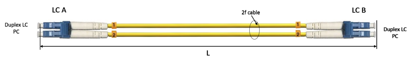
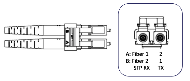
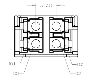
Single-mode Duplex LC PC to Duplex LC PC Optical Connector
The fiber which connects connector A lane 1 must end at connector B lane 2 at the other end of the link.
Duplex LC to Duplex LC Patch Cable Fiber Connections:
|
Connector A Duplex LC |
Connection |
Connector B Duplex LC |
|
1 |
------> |
2 |
|
2 |
<------ |
1 |
Multiple Duplex LC patch cables can be connected in series, but each added connector pair adds reflections in the link which impairs performance.
Typical Single Mode Duplex LC Fiber Patch Cable:
Back shell Label
The label applied on the transceiver's back-shell is illustrated below. Note that the Images are for illustration purposes only. Labels look and placement may vary.
Transceiver Label (Illustration)
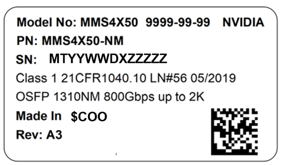
Images are for illustration purposes only. Product labels, colors, and form may vary.
Transceiver Back-Shell Label Serial Number Legend
|
Symbol |
Meaning |
Notes |
|
MT |
Manufacturer name (Mellanox Technologies) |
2 digits (alphanumeric) |
|
YY |
Year of manufacturing |
2 last digits of the year (numeric) |
|
WW |
Week of manufacturing |
2 digits (numeric) |
|
JC or DM |
Manufacturer Site: JC – Option 1 (China) DM – Option 2 (Malaysia) |
Two characters |
|
SSSSS |
Serial number |
5 digits (decimal numeric) for serial number, starting from 00001. |
Regulatory Compliance
The transceiver is a Class 1 laser product. It is certified per the following standards:
|
Feature |
Agency |
Standard |
|
Laser Eye Safety |
FDA/CDRH |
CDRH 21 CFR 1040 and Laser Notice 50 |
|
Electrical Safety |
CB |
IEC 62368 |
|
Electrical Safety |
UL/CSA |
UL 62368 and CAN/CSAN 62368 |
Handling and Cleaning
The transceiver can be damaged by exposure to current surges and over voltage events. Take care to restrict exposure to the conditions defined in Absolute Maximum Ratings. Observe normal handling precautions for electrostatic discharge-sensitive devices.
The transceiver is shipped with dust caps on both the electrical and the optical port. The cap on the optical port should always be in place when there is no fiber cable connected. The optical connector has a recessed connector surface which is exposed whenever it has no cable nor cap.
Important note 1: Keep both the fiber and transceiver dust caps.
Important note 2: Clean both transceiver receptacle and cable connector prior to insertion of the fiber cable, to prevent contamination from it.
The dust cap ensures that the optics remain clean during transportation. Standard cleaning tools and methods should be used during installation and service. Liquids must not be applied.
Important note 3: 80% of transceiver link problems are related to dirty optical connectors.