Open topic with navigation
Overview
The data cache hierarchy of CUDA devices is described in the Programming Guide's compute capability sections, e.g. 2.x and 3.x. In general, there are three types of data caches: L1, L2, and texture. Loads from the caches are made via transactions of a fixed size. L1 transactions are 128 bytes, and L2 and texture transactions are 32 bytes. An important strategy for optimizing memory usage is to group loads and stores in order to access the necessary data in as few cache transactions as possible. For memory cached in both L1 and L2, if every thread in a warp loads a 4-byte value from sparse locations which miss in L1 cache, each thread will incur one 128-byte L1 transaction and four 32-byte L2 transactions. This will cause the load instruction to reissue 32 times more than if the values would be adjacent and cache-aligned. If bandwidth between caches becomes a bottleneck, rearranging data or algorithms to access the data more uniformly can alleviate the problem. See the Global Memory sections of the Programming Guide for more details.
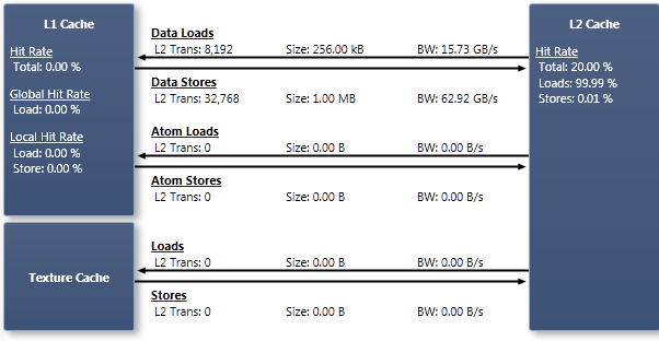
Chart

Caches
Global memory accesses are routed either through L1 and L2, or only L2, depending on the architecture and the type of instructions used. Global read-only memory accesses are routed through the texture and L2 caches. See the Memory Statistics Global experiment for an explanation of how to control whether global accesses bypass L1. Local memory is routed through L1 and L2 cache. See the Memory Statistics Local experiment for more information on local memory accesses. Texture memory is read-only device memory, and is routed through the texture cache and the L2 cache. See the Memory Statistics Texture experiment for details on texture accesses. Shared memory accesses do not go through any cache.
|
Analysis
-
If the L1 Cache Hit Rate is low …
-
… first check to see if the L1 cache is being used. Some devices and some types of memory instructions bypass L1 cache.
-
… check to see if caching mode is PREFER_L1. If not, increasing the L1 cache size can help improve the hit rate. Note that increasing L1 cache size requires decreasing the shared memory size, so this is only a valid option if the kernel does not need the extra shared memory.
-
… the access pattern is not a good match for the L1 cache's optimizations for linear locality. Try to modify the access patterns to group accesses more closely together. Alternatively, for 2D access patterns, texture memory may be more efficient than global memory.
-
… if the bandwidth between L1 and L2 is a bottleneck, and the L1 transactions per request ratio is high, consider changing accesses to bypass L1 and go directly to L2. Since each L1 miss incurs four L2 transactions, going directly to L2 can result in up to 75% less L2 bandwidth needed to access the data. See the Memory Statistics Global experiment's Overview section for information on changing reads to bypass L1.
-
… try to reduce register spilling by increasing the registers per thread.
NVIDIA GameWorks Documentation Rev. 1.0.150630 ©2015. NVIDIA Corporation. All Rights Reserved.
