Jetson Thor Adaptation and Bring-Up#
This guide describes how to port and bring up custom platforms using the NVIDIA® Jetson™ T5000 module, based on the NVIDIA Jetson Linux Driver Package.
The examples in this document include code for the Jetson T5000 module and the Jetson Thor carrier board.
For information about customizing the configuration files, refer to the T26x BCT (Boot Configuration Table) Deployment Guide.
Board Configuration#
The Jetson Thor P3834 is a System on Module (SOM), and it is pin compatible with the Jetson AGX Thor Developer Kit carrier board P4071. This section uses that combination to illustrate how end users can use a custom-designed carrier board for this module. The SOM has an EEPROM in which the board ID and system-level details are saved, and the SOM can be used without any software configuration modifications.
The SOM that is to be incorporated with customer products has a thermal transfer plate (TTP) that is ready to accept a customer-provided thermal solution.
Before you use the SOM with a carrier board other than P4071, change the kernel device tree, the MB1 configuration, the MB2 configuration, the ODM data, and the flashing configuration to correspond to the new carrier board instead of the P4071. The next section provides more information about the changes.
Name the Board#
To support a SOM with your carrier board, you must assign a lowercase alphanumeric name to the module and carrier board combination. The name can include hyphens (-) and underscores (_) but not spaces. Two examples of valid names are as follows:
p4070-0000-devkit
devboard
The name you select appears in
File names and paths.
User-visible device-tree file names.
This name is also exposed to the user through various Linux kernel proc files.
Note
In this section, <board> represents your board name.
You must also select a similarly constructed vendor name, and the same character set rules apply. The following is an example:
nvidia
Note
In this section, <vendor> represents your vendor name.
Placeholders in the Porting Instructions#
Placeholders are used throughout this topic. When executing commands, substitute an appropriate value for each placeholder.
<function>is a functional module name, which might bepower-tree,pinmux,sdmmc-drv,keys,comm(Wi-Fi/Bluetooth®),camera, and so on.<board>is the name you selected to represent your platform.For example,
P4071is the name of the Jetson AGX Thor Developer Kit. The NVIDIA board names use lowercase letters.<version>is a board version number, such asa00.Files for NVIDIA reference boards include a version number. Files for customer platforms are not required to include a version number.
<vendor>is the name of your organization or the name of the vendor for your board.
Root Filesystem Configuration#
Jetson Linux can use any standard or customized Linux root filesystem (rootfs) that is appropriate for its targeted embedded applications. However, some settings must be configured in the rootfs boot-up framework to set the default configuration after the boot; otherwise, some of the core functionalities will not run as expected.
For example:
The
nv.shandnvfb.shboot-up scripts complete some platform-specific configurations in the kernel.The Xorg and X libraries must be correctly configured for the target device.
The nvpmodel clock and frequency must be configured for the target device.
MB1 Configuration Changes#
Starting in version T264, multiple .dts/.dtsi files define the boot time configuration of the hardware. These files are applied by the Bootloader. The MB1 boot configuration tables are available in the following location:
``<l4t_top>/bootloader/generic/BCT``
Generate the Pinmux dtsi Files#
To define your board’s pinmux configuration, download the Jetson Thor pinmux table from the Jetson Download Center. The table is a spreadsheet that provides the following information:
The locations and default pinmux settings.
The pinmux settings definitions, which are in the source code or device tree.
To access the spreadsheet:
Go to Jetson Download Center.
Search for Thor Series Pinmux and download the spreadsheet.
Before you open the spreadsheet, ensure that macros are enabled.
Ensure that the Pin Direction column is consistent with the selected peripheral function.
For example, I2C pins (clock and data) are bidirectional signals.
The Req Initial State should be consistent with the direction.
For example, the Drive 1 and Drive 0 options are applicable only to the output and bidirectional modes.
The 3.3V Tolerance option is available only for certain pins.
When you enable this option, that pin functions as an open drain.
Customize the spreadsheet to configure your board, and click Generate DT File to generate the following files:
gpio.dtsipadvoltage.dtsipinmux.dtsi
Note
The names of the generated files depend on the input you provided during Generate DT File.
Copy the
gpio.dtsi,padvoltage.dtsi, andpinmux.dtsifiles to the<l4t_top>/bootloader/directory.Rename the GPIO header file in
pinmux.dtsito the correctgpio.dtsifile name.
After copying the files, ensure that you point these files to the new board.conf file that you created for your board. For more information, refer to Flash the Build Image.
Change the Pinmux#
The pinmux configuration can be changed in one of the following ways:
Update the MB1 pinmux BCT as mentioned in Generate the Pinmux dtsi Files.
For debugging, you can dynamically change the pinmux.
To dynamically change the pinmux:
Get the pinmux register address.
In TRM, click System Components → Multi-Purpose I/O Pins and Pin Multiplexing (PinMux) → Pinmux Registers.
Search for the pin name (for example,
SOC_GPIO130).Write down the complete pin name (for example,
PADCTL_G3_SOC_GPIO130_0) and the offset (for example,SOC_GPIO130: Offset = 0x30).
#. Go to the Jetson Thor Technical Reference Manual and, in Table 1-15: Pad Control Grouping, find the
G3 pad control block = PADCTL_A0entry.On the Memory Architecture page, click Memory Mapped I/O → Address Map.
Search for PADCTL_A0.
The base address is PADCTL_A0 = 0x810c282000, and the pinmux register address is PADCTL base address + offset.
For example,
SOC_GPIO130 Pinmux register address = 0x810c282000 + 0x30 = 0x810c282030.
Get the current register value in the device by using the devmem tool.
Install devmem:
$ sudo apt-get install busybox
Run devmem, specifying the pinmux register address:
$ busybox devmem <64-bit address>
For example, devmem 0x810c282030.
To use the pin as GPIO, update the following fields in the PADCTL register. Find register information from the Pinmux Registers section in the TRM as mentioned in step 2.
Set GPIO to Bit 10 = 0.
For the output, set Bit 4 = 0; Bit 6 = 0.
For the input, set Bit 4 = 1; Bit 6 = 1.
Use the devmem tool to set the register; for example,
busybox devmem 0x810c282030 w 0x00203050.Verify that the register value is set correctly.
Example
To update Pin MCLK05: SOC_GPIO130: PL.06:
Adjust the pinmux to map the pin to GPIO.
Configure the GPIO controller (input, output high, or output low).
The pinmux register base address is 0x810c282000 and the offset is 0x30, so the pinmux register address is 0x810c282030.
To configure the pinmux for this pin:
Run the following command:
$ busybox devmem 0x810c282030
The output value is 0x00203401.
To set the pin as the output, run the following command:
$ busybox devmem 0x810c282030w 0x00203000
To confirm, check the output:
$ busybox devmem 0x810c282030
Starting with JetPack 6, the GPIO sysfs is deprecated.
To set the direction of the GPIO controller between the input and the output, users can use upstream GPIO tools instead of GPIO sysfs.
Identify and Use GPIO Pins#
If you designed your own carrier board to translate from the SOM connector pins to actual GPIO numbers, you must understand the following GPIO mapping formula. The translated GPIO numbers can be controlled by the driver.
You can check the GPIO number using Kernel debugfs.
Search for the GPIO pin in the Jetson AGX Thor pinmux table (refer to Generate the Pinmux dtsi Files).
For example,
SOC_GPIO170, which is GPIO3_PU.00.Follow the GPIO debugfs lookup that uses the port and offset:
$ cat /sys/kernel/debug/gpio \| grep PU.00
The GPIO number is mentioned in the first column as gpio-356.
After identifying the GPIO number, you can use the gpiod utility to configure the pin as input or output. For more information, refer to Using the Pins in GPIO Mode.
Note
To use a pin as the GPIO, ensure that the E_IO_HV field is disabled in the corresponding pinmux register of the GPIO pin. You can disable the 3.3V Tolerance Enable field in the pinmux spreadsheet and reflash the board with the updated pinmux file.
MB2 Configuration Changes#
Modifying for EEPROM#
EEPROM is an optional component for a customized carrier board. If the carrier board is designed without an EEPROM, the following modifications are needed on the MB2 BCT file, Linux_for_Tegra/bootloader/generic/BCT/tegra264-mb2-bct-common.dtsi:
- cvb_eeprom_read_size = <0x100>
+ cvb_eeprom_read_size = <0x0>
Port the Linux Kernel Device Tree Files#
This section assumes that the P3834 SOM is connected to a P4071 carrier board and the board has not been modified. Based on the peripherals on your carrier board, you can modify the .dts files by disabling or enabling the controllers and changing the power supplies. This section provides details and suggestions for the porting exercise.
To port the kernel configuration code or the device tree to your platform, modify one of the distributed configuration files to describe the design of your platform.
The configuration files can be downloaded (refer to Obtaining the Kernel Sources) and are available in the following directories:
<top>/hardware/nvidia/platform/t264/<top>/hardware/nvidia/t264/nv-public
The final DTB file that is used is generated from the tegra264-p4071-0080+p3834-0008-qspi-ufs-nvme.dts source device tree (DT) file:
tegra264-p4071-0080+p3834-0008-qspi-ufs-nvme.dtb
By reading the source DT file, you see the other .dtsi files that are referenced by the include statements, specifically the tegra264-p4071-0000.dtsi file, and the display node includes the tegra264-p4071-0080-p3834-0008-dcb.dtsi file. For more information about the display panel and node, refer to Display Configuration and Bring-up. The tegra264-p4071-0000.dtsi file represents the carrier board (in this case, P4071 with specific hardware design changes) and can serve as a guide for end users to implement .dts and .dtsi files based on their custom carrier boards.
As a general practice, end users can take the existing tegra264-p4071-0000.dtsi file as a starting point.
Note
Use dtc to generate a .dts file from the final .dtb file and verify that your changes have taken effect.
The example command usage is as follows:
dtc -I dtb -O dts tegra264-p4071-0080+p3834-0008-qspi-ufs-nvme.dtb > example.dts
Enable 25-Gigabit Ethernet on QSFP Port#
In the Jetson AGX Thor Developer Kit, the QSFP port can support both 10 Gigabit Ethernet (10GbE) and 25 Gigabit Ethernet (25GbE). The default is 10GbE. The QSFP port can support only one configuration at a time. To enable 25GbE, apply the following patches, rebuild the BSP, and flash the device.
Update the kernel device tree by patching Linux_for_Tegra/kernel/dtb/tegra264-p4071-0000+p3834-0008-nv.dtb:
diff --git a/nv-platform/tegra264-p4071-0000.dtsi b/nv-platform/tegra264-p4071-0000.dtsi
index 936b556..317d59d 100644
--- a/nv-platform/tegra264-p4071-0000.dtsi
+++ b/nv-platform/tegra264-p4071-0000.dtsi
@@ -219,8 +219,7 @@
     mgbe0: ethernet@a808a10000 {
      status = "okay";
      nvidia,mac-addr-idx = <1>;
-        nvidia,uphy-gbe-mode = <1>;
-        nvidia,phy-iface-mode = <0x0>;
+        nvidia,uphy-gbe-mode = <2>;
         nvidia,max-platform-mtu = <9000>;
         nvidia,pcs-rx-eq-sw-ovrd = <1>;
         nvidia,pps_op_ctrl = <8>;
@@ -228,7 +227,7 @@
         fixed-link {
          full-duplex;
-            speed = <10000>;
+            speed = <25000>;
         };
     };
@@ -236,8 +235,7 @@
      mgbe1: ethernet@a808b10000 {
      status = "okay";
      nvidia,mac-addr-idx = <2>;
-     nvidia,uphy-gbe-mode = <1>;
-     nvidia,phy-iface-mode = <0x0>;
+     nvidia,uphy-gbe-mode = <2>;
      nvidia,max-platform-mtu = <9000>;
      nvidia,pcs-rx-eq-sw-ovrd = <1>;
      nvidia,pps_op_ctrl = <8>;
@@ -245,7 +243,7 @@
      fixed-link {
          full-duplex;
-         speed = <10000>;
+         speed = <25000>;
         };
     };
@@ -253,8 +251,7 @@
      mgbe2: ethernet@a808d10000 {
      status = "okay";
      nvidia,mac-addr-idx = <3>;
-     nvidia,uphy-gbe-mode = <1>;
-     nvidia,phy-iface-mode = <0x0>;
+     nvidia,uphy-gbe-mode = <2>;
      nvidia,max-platform-mtu = <9000>;
      nvidia,pcs-rx-eq-sw-ovrd = <1>;
      nvidia,pps_op_ctrl = <8>;
@@ -262,7 +259,7 @@
      fixed-link {
          full-duplex;
-         speed = <10000>;
+         speed = <25000>;
         };
     };
@@ -270,8 +267,7 @@
      mgbe3: ethernet@a808e10000 {
      status = "okay";
      nvidia,mac-addr-idx = <4>;
-     nvidia,uphy-gbe-mode = <1>;
-     nvidia,phy-iface-mode = <0x0>;
+     nvidia,uphy-gbe-mode = <2>;
      nvidia,max-platform-mtu = <9000>;
      nvidia,pcs-rx-eq-sw-ovrd = <1>;
      nvidia,pps_op_ctrl = <8>;
 @@ -279,7 +275,7 @@
      fixed-link {
          full-duplex;
-            speed = <10000>;
+            speed = <25000>;
         };
     };
Build the DTB and replace it in the following paths:
Linux_for_Tegra/kernel/dtb/tegra264-p4071-0000+p3834-0008-nv.dtb
Linux_for_Tegra/rootfs/boot/tegra264-p4071-0000+p3834-0008-nv.dtb
Linux_for_Tegra/bootloader/tegra264-p4071-0000+p3834-0008-nv.dtb
Update Linux_for_Tegra/bootloader/generic/tegra264-bpmp-3834-0008-4071-xxxx.dtb as follows:
--- a/tegra264-bpmp-3834-0008-4071-xxxx.dts
+++ b/tegra264-bpmp-3834-0008-4071-xxxx.dts
@@ -68,15 +68,15 @@
  *
  *   UPHY1
  *   Option | Lane 0 | Lane 1 | Lane 2 | Lane 3 |        Lane 4   |      Lane 5      |        Lane 6    |      Lane 7     |
- *      7   |          PCIE C5 x4 (DM)          |     MGBE0 10G   |     MGBE1 10G    |      MGBE2 10G   |     MGBE3 10G   |
+ *      8   |          PCIE C5 x4 (DM)          |     MGBE0 25G   |     MGBE1 25G    |      MGBE2 25G   |     MGBE3 25G   |
  */
  status = "okay";
  uphy0-config = <7>;      // Configure UPHY0-Lane6-7 for UFS
-       uphy1-config = <7>;      // Configure UPHY1-Lane0-3 for C5 to enable mgbe
-       mgbe0-speed = <2>;       /* 0 for 2.5G, 1 for 5G, 2 for 10G, 3 for 25G */
-       mgbe1-speed = <2>;       /* 0 for 2.5G, 1 for 5G, 2 for 10G, 3 for 25G */
-       mgbe2-speed = <2>;       /* 0 for 2.5G, 1 for 5G, 2 for 10G, 3 for 25G */
-       mgbe3-speed = <2>;       /* 0 for 2.5G, 1 for 5G, 2 for 10G, 3 for 25G */
+       uphy1-config = <8>;      // Configure UPHY1-Lane0-3 for C5 to enable mgbe
+       mgbe0-speed = <3>;       /* 0 for 2.5G, 1 for 5G, 2 for 10G, 3 for 25G */
+       mgbe1-speed = <3>;       /* 0 for 2.5G, 1 for 5G, 2 for 10G, 3 for 25G */
+       mgbe2-speed = <3>;       /* 0 for 2.5G, 1 for 5G, 2 for 10G, 3 for 25G */
+       mgbe3-speed = <3>;       /* 0 for 2.5G, 1 for 5G, 2 for 10G, 3 for 25G */
};
nvtherm {
Build the BPMP DTB and copy it to the following locations:
Linux_for_Tegra/bootloader/generic/tegra264-bpmp-3834-0008-4071-xxxx.dtb
Linux_for_Tegra/bootloader/tegra264-bpmp-3834-0008-4071-xxxx.dtb
Reflash the board
Configure the PCIe Controller#
PCIe Controller Features#
Note
Not all controllers are available for user access in the Jetson T5000 module.
Jetson Thor has PCIe controllers with the following specifications:
Speed: All controllers support up to Gen5 speed.
Lane width
C4: up to x8.
C1, C2, C5: up to x4.
C3: up to x2.
Controllers: Controllers C2, C4, and C5 support dual mode; that is, they can be configured as endpoints.
ASPM: All controllers support ASPM.
Enable PCIe in a Customer CVB Design#
Enable the respective controller’s BPMP DT node by adding the property
status = "okay";.The default PCIe mode is set to Root Port. If required, change the mode to Endpoint by adding the
pcie-mode = <2>;property in the BPMP DT node.Enable the respective controller’s kernel DT node by adding the property
status = "okay";.Configure the PCIe reset (
PEX_L*_RST_N) and clkreq (PEX_L*_CLKREQ_N) as follows. To update the pinmux value, refer to Change the Pinmux.
Pinmux setting for Root Port mode:
Pinmux |
Customer Usage |
Pin Direction |
3.3V Tolerance Enable |
|---|---|---|---|
PEX_L*_RST_N |
SFIO(PE*_RST_L) |
Output |
Enable |
PEX_L*_CLKREQ_N |
SFIO(PE*_CLKREQ_L) |
Bidirectional |
Enable |
Pinmux setting for Endpoint mode:
Pinmux |
Customer Usage |
Pin Direction |
3.3V Tolerance Enable |
|---|---|---|---|
PEX_L*_RST_N |
GPIO(rsvd1) |
Input |
Enable |
PEX_L*_CLKREQ_N |
SFIO(PE*_CLKREQ_L) |
Bidirectional |
Enable |
Note
PCIe RP and EP are mutually exclusive; either RP node or EP node can be enabled at a time.
PCIe controller DT nodes:
PCIe Controller and Mode |
PCIe Controller DT Node |
BPMP DT Node |
|---|---|---|
PCIe C0 RP |
pcie@0 |
|
PCIe C1 RP |
pcie@1 |
|
PCIe C2 RP |
pcie@2 |
|
PCIe C3 RP |
pcie@3 |
|
PCIe C4 RP |
pcie@4 |
|
PCIe C5 RP |
pcie@5 |
|
PCIe C2 EP |
pcie@2 |
|
PCIe C4 EP |
pcie@4 |
|
PCIe C5 EP |
pcie@5 |
The following example shows PCIe x8 (C4) in Root Port mode:
bpmp-dt
diff --git a/tegra264-bpmp-3834-0008-4071-xxxx.dts b/tegra264-bpmp-3834-0008-4071-xxxx.dts
index eace560..74bb9b3 100644
--- a/tegra264-bpmp-3834-0008-4071-xxxx.dts
+++ b/tegra264-bpmp-3834-0008-4071-xxxx.dts
@@ -53,10 +53,10 @@
                        status="disabled";
                };
                pcie@4{
-                       status="disabled";
+                       status="okay";
                };
                pcie@5{
-                       status="okay";
+                       status="disabled";
                };
        };
kernel-dt
diff --git a/nv-platform/tegra264-p4071-0000.dtsi b/nv-platform/tegra264-p4071-0000.dtsi
index 8d9a23f..4f304c6 100644
--- a/nv-platform/tegra264-p4071-0000.dtsi
+++ b/nv-platform/tegra264-p4071-0000.dtsi
@@ -290,12 +290,12 @@
                pcie@a808460000 {
-                       status = "disabled";
+                       status = "okay";
                };
               pcie@a808480000 {
-                       status = "okay";
+                       status = "disabled";
                };
                padctl@a808680000 {

pinmux
diff --git a/jedha/pinmux/tegra264-mb1-bct-pinmux-p3834-xxxx-p4071-0000.dtsi b/jedha/pinmux/tegra264-mb1-bct-pinmux-p3834-xxxx-p4071-0000.dtsi
index 6ca44a4..a184ede 100644
--- a/jedha/pinmux/tegra264-mb1-bct-pinmux-p3834-xxxx-p4071-0000.dtsi
+++ b/jedha/pinmux/tegra264-mb1-bct-pinmux-p3834-xxxx-p4071-0000.dtsi
@@ -2130,10 +2130,10 @@ pinmux@ac281000 {
                        pex_l4_clkreq_n_pd0 {
                                nvidia,pins = "pex_l4_clkreq_n_pd0";
-                               nvidia,function = "rsvd1";
-                               nvidia,pull = <TEGRA_PIN_PULL_DOWN>;
-                               nvidia,tristate = <TEGRA_PIN_ENABLE>;
-                               nvidia,enable-input = <TEGRA_PIN_DISABLE>;
+                               nvidia,function = "pe4_clkreq_l";
+                               nvidia,pull = <TEGRA_PIN_PULL_NONE>;
+                               nvidia,tristate = <TEGRA_PIN_DISABLE>;
+                               nvidia,enable-input = <TEGRA_PIN_ENABLE>;
                                nvidia,drv-type = <TEGRA_PIN_1X_DRIVER>;
                                nvidia,e-io-od = <TEGRA_PIN_ENABLE>;
                                nvidia,e-lpbk = <TEGRA_PIN_DISABLE>;
@@ -2141,9 +2141,9 @@ pinmux@ac281000 {
                        pex_l4_rst_n_pd1 {
                                nvidia,pins = "pex_l4_rst_n_pd1";
-                               nvidia,function = "rsvd1";
-                               nvidia,pull = <TEGRA_PIN_PULL_DOWN>;
-                               nvidia,tristate = <TEGRA_PIN_ENABLE>;
+                               nvidia,function = "pe4_rst_l";
+                               nvidia,pull = <TEGRA_PIN_PULL_NONE>;
+                               nvidia,tristate = <TEGRA_PIN_DISABLE>;
                                nvidia,enable-input = <TEGRA_PIN_DISABLE>;
                                nvidia,drv-type = <TEGRA_PIN_1X_DRIVER>;
                                nvidia,e-io-od = <TEGRA_PIN_ENABLE>;
Debug PCIe Link-Up Failure#
After you make the required device tree changes, as mentioned in Enable PCIe in a Customer CVB Design, if the PCIe link fails to come up, complete the following debug steps to triage the issue.
Add the following patch to the bpmp-fw dtb:
diff --git a/include/pcie/pcie-common.dtsi b/include/pcie/pcie-common.dtsi
index 0edfca7df9a5..9ff46be749ba 100644
--- a/include/pcie/pcie-common.dtsi
+++ b/include/pcie/pcie-common.dtsi
@@ -23,6 +23,7 @@
                        pcie-id = <1>;
                        pcie-mode = <1>;
                        max-link-speed = <5>;
+                       hot-plug-capable = <1>;
                };
                pcie@2 {
@@ -30,6 +31,7 @@
                        pcie-id = <2>;
                        pcie-mode = <1>;
                        max-link-speed = <5>;
+                       hot-plug-capable = <1>;
                };
                pcie@3 {
@@ -37,6 +39,7 @@
                        pcie-id = <3>;
                        pcie-mode = <1>;
                        max-link-speed = <5>;
+                       hot-plug-capable = <1>;
                };
                pcie@4 {
@@ -44,6 +46,7 @@
                        pcie-id = <4>;
                        pcie-mode = <1>;
                        max-link-speed = <5>;
+                       hot-plug-capable = <1>;
                };
                pcie@5 {
@@ -51,6 +53,7 @@
                        pcie-id = <5>;
                        pcie-mode = <1>;
                        max-link-speed = <5>;
+                       hot-plug-capable = <1>;
                };
        };
};
After you add this patch, lspci should list the Root Port device as follows:
$ lspci
00:01.0 PCI bridge: NVIDIA Corporation Device 10e5 (rev a1)
To triage from the platform side, ensure that signal routing exists from Root Port to Endpoint:
PERST# routing: Verify that it goes high when Root Port attempts the linkup.
CLKREQ# routing: By default, ASPM is disabled, so this routing has no role in linkup failure. If you enabled ASPM L1-CPM or L1SS by completing the steps in Enable the PCIe ASPM, verify whether this pulled low when Root Port attempts the linkup.
REFCLK routing: Ensure that REFCLK flows from Root Port to Endpoint. Connect the scope and observe the spread-enabled 100 MHz clock.
Tx and Rx routing: Verify that Tx and Rx lanes routing are fine.
Tip
If any of the preceding signals go through board-level muxes, verify that those muxes are configured correctly.
PCIe slot regulators or GPIOs: If PCIe slot regulators are present, verify that they are powered up. If the endpoint expects some GPIO signals to be toggled as part of the power-up sequence, verify that it is happening. For example, some Wi-Fi cards expect the
WDISABLE_1signal to be asserted before PCIe linkup.
To triage from the software side:
Verify DLActive status in Root Port LnkSta of
lspci -vvvoutput. This is to check whether the link comes up by the time kernel boots to shell (for example, to confirm whether the link is taking more time than usual to come up).Dump
PADCTL_PEX_CTL_PEX_L*_CLKREQ_N_0andPADCTL_PEX_CTL_PEX_L*_RST_N_0pinmux values and verify that the settings are correct.Dump the
NV_XPL_PL_LTSSM_STATE_0register. (For the register address of each controller, refer to the TRM.) Accessing the controller’s address, which is not enabled, will cause a CBB power down error. When you share this information in the NVIDIA developer forum, it helps us determine the LTSSM state.Reduce the link speed to Gen-1 using the
max-link-speeddevice tree properties in thebpmp-fwDTB.
Enable the PCIe ASPM#
To enable the desired ASPM state, set the respective bit in the aspm-capability DT property in the bpmp-fw DTB. The following ASPM states are represented by each bitfield:
#define PCIE_ASPM_DISABLE  0x00U
#define PCIE_ASPM_L1       0x02U
#define PCIE_ASPM_L11      0x04U
#define PCIE_ASPM_L12      0x08U
#define PCIE_ASPM_L1_PLLPD 0x10U
#define PCIE_ASPM_L1_CPM   0x20U
#define PCIE_ASPM_ALL      (PCIE_ASPM_L1 | PCIE_ASPM_L11 | PCIE_ASPM_L12 | PCIE_ASPM_L1_PLLPD | PCIE_ASPM_L1_CPM)
Execute the appropriate command to enable or disable the respective ASPM state.
To enable L1:
echo powersave > /sys/module/pcie_aspm/parameters/policy
To enable L1 and L1SS:
echo powersupersave > /sys/module/pcie_aspm/parameters/policy
To disable ASPM:
echo performance > /sys/module/pcie_aspm/parameters/policy
Confirm the status of the various ASPM states from the lspci -vvv output and dump the following registers to check the ASPM state entry count:
-  ``NV_XPL_PL_LTSSM_L1_ENTRY_COUNT_0``
-  ``NV_XPL_PL_LTSSM_L1_CPM_ENTRY_COUNT_0``
-  ``NV_XPL_PL_LTSSM_L1_1_ENTRY_COUNT_0``
-  ``NV_XPL_PL_LTSSM_L1_2_ENTRY_COUNT_0``
Port the Universal Serial Bus#
Jetson Thor can support up to four enhanced SuperSpeed Universal Serial Bus (USB) ports. In some implementations, not all of these ports can be used because of Universal Physical Layer (UPHY) lane sharing among PCIe, UFS/NVME, and XUSB. The Jetson P4071 carrier board can support three USB ports. If you designed your carrier board, verify the UPHY lane mapping and compatibility between P4071 and your custom board by consulting the NVIDIA team.
USB Structure#
An enhanced SuperSpeed USB port has nine pins:
VBUS.
GND.
D+.
D−.
Two differential signal pairs for SuperSpeed data transfer.
One ground (GND_DRAIN) for drain wire termination and managing EMI, RFI, and signal integrity.

The D+ and D− signal pins connect to UTMI pads. The SSTX and SSRX signal pins connect to UPHY and are handled by one UPHY lane. UPHY lanes are shared among PCIe, UFS, and XUSB. The UPHY lanes must be assigned based on the custom carrier board’s requirements.
Universal Physical Layer Lane Assignment#
UPHY is a physical I/O interface layer that can serve multiple types of interfaces, such as USB and PCIe. A UPHY lane can support multiple interface types.
The Jetson P4071 carrier board USB ports have the following UPHY lanes:
Jetson SODIMM Signal Name |
Jetson Thor UPHY Block and Lane |
Jetson Thor Function |
|---|---|---|
UPHY_RX0/TX0 |
UPHY0, Lane 0 |
USB 3.1 (P0) |
UPHY_RX1/TX1 |
UPHY0, Lane 1 |
USB 3.1 (P1) |
UPHY_RX2/TX2 |
UPHY0, Lane 2 |
USB 3.1 (P2) |
Note
Before you design your custom board, refer to the Jetson Thor Technical Reference Manual and the NVIDIA Jetson AGX Thor Series Product Design Guide (DG), and then contact NVIDIA.
Required Device Tree Changes#
This section provides guidance about checking schematics and configuring USB ports in the device tree. The examples are based on the P3834 SOM and P4071 carrier board.
For a Host-Only Port#
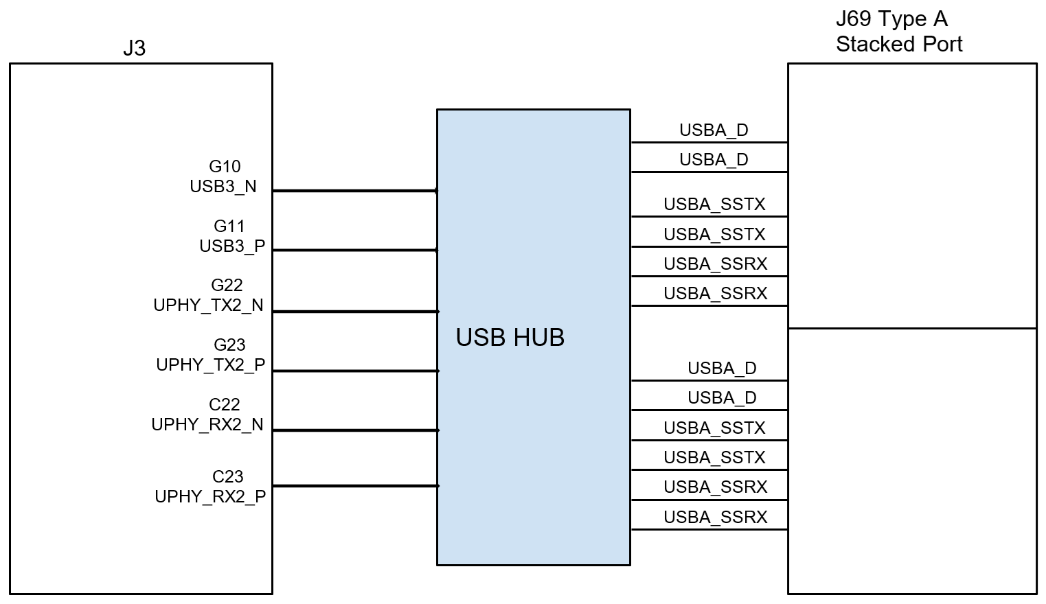
This section uses a J69 type A stacked connector as an example of a host-only port. The USB signals (USB 2.0 and USB 3.2) for the J3 come from the Port 0 USBSS lines of the SOM through the USB hub, as shown in the following diagram.
The xusb_padctl Node#
The xusb_padctl node of the device tree follows the conventions of the pinctrl-bindings.txt kernel document. It contains two sets of nodes named pads and ports, which describe the USB2 and USB3 signals with parameters and port numbers. The name of each parameter description subnode in pads and ports must be in the form <type>-<port_number>, where <type> is usb2 or usb3 and <port_number> is the associated port number.
The pads Subnode#
nvidia,function: A string that contains the name of the function to mux to the pin or group.The value must be
xusb.
The ports Subnode#
mode: A string that describes the USB port capability.A port for USB2 must have this property, and it must be one of the following values:
hostdeviceOTG
nvidia,usb2-companion: USB2 port (0/1/2/3) to which the port is mapped.A port for USB3 must have this property.
nvidia,oc-pin: The overcurrent VBUS pin that the port is using.The value must be positive or zero.
Note
Some Type-C port controllers, such as from Cypress, can handle the overcurrent detection and handling. Therefore, you do not need to set this property for USB Type-C connectors that have Type-C port controllers.
vbus-supply: VBUS regulator for the corresponding UTMI pad.Set to
&battery_regfor a dummy regulator. This value is needed when the VBUS line is controlled by PD controllers and for Type-C connectors and ports.For detailed information about
xusb_padctl, refer to the following kernel documentation:kernel/3rdparty/canonical/linux-noble/Documentation/devicetree/bindings/phy/nvidia,tegra194-xusb-padctl.yaml
Example: USB Port Enablement for xusb_padctl#
Using J69 (Type-A stacked port) as an example, create a pad/port node and property list:
xusb_padctl: padctl@a808680000 {
    ...
    pads {
        usb2 {
            lanes {
                ...
                usb2-3 {
                    nvidia,function = "xusb";
                    status = "okay";
                };
                ...
            };
        };
    };
    usb3 {
        lanes {
            ...
            usb3-2 {
                nvidia,function = "xusb";
                status = "okay";
            };
            ...
        };
    };
ports {
    ...
        usb2-3 {
            mode = "host";
            status = "okay";
        };
        ...
    };
};
Under the xHCI Node#
The Jetson Thor xHCI controller complies with xHCI specifications, which support the USB 2.0 high-speed, full-speed, and low-speed protocols and the USB 3.2 SuperSpeed protocol.
phys: Must contain an entry for each entry inphy-names.phy-names: Must include an entry for each PHY used by the controller.The names must be of the form
<type>-<port_number>, where<type>isusb2orusb3.nvidia,xusb-padctl: A pointer to thexusb-padctlnode.
For more information, refer to the following kernel documentation:
kernel/3rdparty/canonical/linux-noble/Documentation/devicetree/bindings/usb/nvidia,tegra234-xusb.yaml
Example: USB Port Enablement or tegra_xhci#
This example contains a J69 and creates an xHCI node and property list:
usb@a80aa10000 {
    ...
    phys = <&{/bus@0/padctl@a808680000/pads/usb2/lanes/usb2-3}>,
           <&{/bus@0/padctl@a808680000/pads/usb3/lanes/usb3-2}>;
    phy-names = "usb2-3", "usb3-2";
    nvidia,xusb-padctl = <&xusb_padctl>;
    status = "okay";
    ...
};
For an On-The-Go Port#
USB On-The-Go (OTG), which is often abbreviated as USB OTG or just OTG, is a specification that allows USB to act as a host or a device in the same port. A USB OTG port can toggle between the roles of host and device.
This section takes the J81 and USB3.2 Type-C connector as an example of an OTG port.
An OTG port adds a fifth pin, called the ID pin, to the standard USB connector. An OTG cable has an A-plug on one end and a B-plug on the other end. The ID pin of the A-plug is grounded, and the ID pin of the B-plug is floating. A device with an A-plug inserted becomes an OTG A-device (host), and a device with a B-plug inserted becomes a B-device (device).
Note
The roles of J81, the port switch between the host driver (xHCI) and device driver (xUDC), are controlled by a U286 Cypress Type-C controller and ucsi_ccg driver in the Jetson Thor Developer Kit.
Review the Schematics#
Note
The P4071 carrier board’s schematic file, P4071_A04_Concept_schematics.pdf, is included in the Jetson AGX Thor Series Developer Kit Carrier Board Design Files.
Check the USB connectors on the P4071 carrier board and find the location of the wired socket to P3834.
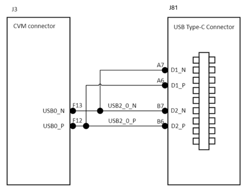
USB 2.0 signal pins D+/D− (USB2_0_*) wire out from J81 and lead to F12 (USB0_P) and F13 (USB0_N) on the SOM socket.
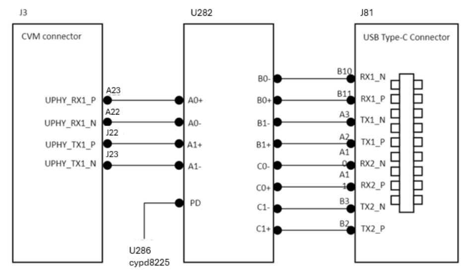
USB 3.2 differential signal pairs (TX* and RX*) wire out from J81 and lead to A22 (UPHY_RX1_N), A23 (UPHY_RX1_P), J22 (UPHY_TX1_N), and J23 (UPHY_TX1_P) on the SOM socket through U282 and U286, the USB Type-C alt mode switch.
Through the schematic, for J81:
The USB 2.0 signal pair is wired to UTMI pad 0 (USB2 port 0).
USB3.2 signal pairs are wired to UPHY lane 1 (USB3.2 port 1 according to UPHY lane mapping).
The USB Connector Class#
A USB connector class represents a physical USB connector. When it is attached to the MUX and USB interface controllers, it should be a child of a USB interface controller or a separate node. Generally, port switching between the roles of an OTG port is controlled by the host driver (xHCI) and device driver (xUDC). You can determine the role by the states of the ID pin and the VBUS_DETECT pin.
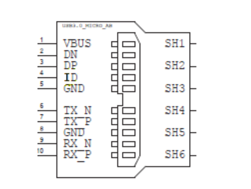
The following example uses GPIO_M3 as the VBUS_DETECT pin and GPIO_Q0 as the ID pin:
Find the corresponding GPIO states on the VBUS_DETECT pin and ID pin.
The ID pin is typically designed as an internal pull high (logical high). With an A-plug connected, the ID pin is pulled to ground (logical low); with a B-plug connected or no cable connected, the pin remains logical high.
The operation of the VBUS_DETECT pin depends on the device’s design. For example, consider the schematic in the following diagram.
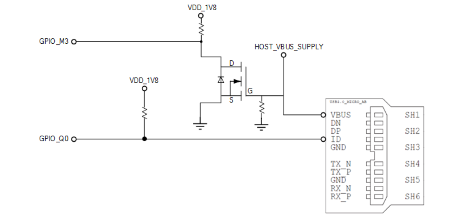
With a B-plug connected, VBUS_DETECT is logical low because VBUS is provided from an external power supply. When no cable is connected, it is logical high.
Note
VBUS_DETECT is initially logical high, and then it is logical low because VBUS is provided by the host controller. Therefore, the state of the VBUS_DETECT pin does not matter when the OTG port is operating in host mode.
Create the table of GPIO states and their corresponding output cable states.
GPIO_Q0 (ID)
GPIO_M3 (VBUS_DETECT)
Data Role
1
1
Not connected
0
0
HOST
0
1
HOST
1
0
DEVICE
Under the Connector Node#
Note
This section is not used on the P4071 carrier board.
Port switching between the roles of an OTG port is defined by the state of the ID pin, the VBUS_DETECT pin, and the settings of the external connector class.
compatible: Value must begpio-usb-b-connector.label: Symbolic name for the connector.type: Size of the connector should be specified to accommodate non-full-size USB-A or USB-B compatible connectors.id-gpios: An input GPIO for the USB ID pin.vbus-gpios: An input GPIO for the USB VBus pin that is used to detect the presence of VBUS 5V.wakeup-source: A Boolean.If the device can wake up the system, the value is
true.For more information about
USBConnectorClass, refer to the following kernel documentation:kernel/3rdparty/canonical/linux-noble/Documentation/devicetree/bindings/connector/usb-connector.yaml
Note
OTG port switching between the host driver (xHCI) and device driver (xUDC) roles is controlled by the Cypress Type-C controller. Therefore, this section is not a part of the device tree for the Jetson AGX Thor Developer Kit.
Create a
USBConnectorClassdevice node and property list based on the device tree structure described earlier and the table of GPIO states and corresponding output cable states for GPIO_Q0 and GPIO_M3:xusb_padctl: padctl@a808680000 { ... ports { usb2-0 { ... Connector { compatible = "gpio-usb-b-connector"; label = "micro-USB"; type = "micro"; vbus-gpio = <&tegra_main_gpio TEGRA194_MAIN_GPIO(M, 3) GPIO_ACTIVE_LOW>; id-gpio = <&tegra_main_gpio TEGRA194_MAIN_GPIO(Q, 0) GPIO_ACTIVE_HIGH>; }; ... }; }; ... };Note
Check the pinmux table for the GPIO that corresponds to the ID pin and VBUS_DETECT pin.
Under the xusb_padctl Node#
The xusb_padctl settings for an OTG port are the same as the settings for a host-only port, except that the mode should be otg. The usb-role-switch property is added, the remote endpoint settings are attached to the CCGx chip, and the bindings of the connector nodes are specified in Documentation/devicetree/bindings/connector/usb-connector.yaml file.
Take J81, which is the USB 3.2 Type-C connector, as an example, and create a pad/port node and property list:
xusb_padctl: padctl@a808680000 {
    ...
    pads {
        usb2 {
            lanes {
                usb2-0 {
                    nvidia,function = "xusb";
                    status = "okay";
                };
                ...
            };
        };
        usb3 {
            lanes {
                ...
                usb3-1 {
                    nvidia,function = "xusb";
                    status = "okay";
                };
                ...
            };
        };
    };
    ports {
        usb2-0 {
            mode = "otg";
            usb-role-switch;
            vbus-supply = <&battery_reg>;
            status = "okay";
            port {
                hs_typec_p1: endpoint {
                    remote-endpoint = <&hs_ucsi_ccg_p1>;
                };
            };
        };
        ...
        usb3-1 {
            nvidia,usb2-companion = <0>;
            status = "okay";
            port {
                ss_typec_p1: endpoint {
                    remote-endpoint = <&ss_ucsi_ccg_p1>;
                };
            };
        };
        ...
    };
};
Under the xHCI Node#
The xHCI settings for an OTG port are the same as the settings for a host-only port.
Take J81, the USB 3.1 Type-C connector, as an example, and create an xHCI node and property list based on the device tree structure described in Under the xHCI Node for a host-only port:
tegra_xhci: usb@a80aa10000 {
    ...
    phys = <&{/bus@0/padctl@a808680000/pads/usb2/lanes/usb2-0}>,
           <&{/bus@0/padctl@a808680000/pads/usb3/lanes/usb3-1}>;
    phy-names = "usb2-0", "usb3-1";
    nvidia,xusb-padctl = <&xusb_padctl>;
    status = "okay";
    ...
};
Under the xUDC Node#
The Jetson AGX Thor xUDC controller supports the USB 2.0 High-Speed/Full-Speed and USB 3.1 SuperSpeed protocols.
charger-detector: USB charger detection support.This protocol must be the phandle of the USB charger detection driver DT node.
phys: An array that must contain a pointer to the node that defines each PHY inphy-names.phy-names: Must include an entry for each PHY used by the controller.The names must be of the form
<type>-<port_number>, where<type>isusb2orusb3.nvidia,xusb-padctl: Must be a pointer to thexusb-padctlnode.For more information about xUDC, refer to the following kernel documentation:
kernel/3rdparty/canonical/linux-noble/Documentation/devicetree/bindings/usb/nvidia,tegra-xudc.txt
Taking J81, which is the USB 3.1 Type-C connector, as an example, create an xUDC node and property list for J81 based on the device tree structure described previously:
usb@a808670000 {
    phys = <&{/bus@0/padctl@a808680000/pads/usb2/lanes/usb2-0}>,
    <&{/bus@0/padctl@a808680000/pads/usb3/lanes/usb3-1}>;
    phy-names = "usb2-0", "usb3-1";
    nvidia,xusb-padctl = <&xusb_padctl>;
    status = "okay";
};
Note
Before designing your custom board, verify the lane mapping by consulting the Jetson AGX Thor OEM Product Design Guide.
Change the Display Port (DP or HDMI)#
The Jetson AGX Thor SOM provides DP or HDMI functionality. The pinmux sheet contains the tab for DP and HDMI. Depending on your custom carrier board design, you should generate the appropriate pinmux files. In addition to pinmux changes, the kernel display dtsi files need to be included in the carrier board kernel DT files. For custom carrier board designs, the following are some of the probable changes.
- DP
- Pinmux table
HPD PIN must be configured as SFIO. (Update pinmux sheet “customer usage” column to “SFIO” or “DP_AUX*”.)
DPAUX lanes must be configured as AUX lanes. (Update pinmux sheet “customer usage” to “DP_AUX_CH*”.)
- Any DCB updates for DP
Update Display Devices > CCB field based on the DPAUX port used for the DP connector.
- Update Display Devices > Type to “DP”.
Update HDMI capable to “0”.
Update connector to the appropriate connector index that has DP connector.
- HDMI
HPD GPIO pin: In the
displaynode, update theos_gpio_hotplug_aproperty with appropriate GPIO pin information.- Pinmux table
HPD PIN must be configured as GPIO. (Update pinmux sheet “customer usage” column as a GPIO.)
DPAUX lanes must be configured as I²C lanes. (Update pinmux sheet “customer usage” to “I2C*”.)
- DCB updates
Update Display Devices > CCB field based on the DPAUX port used for the HDMI connector.
- Update Display Devices > Type to “TMDS”.
Update HDMI capable to “1”.
Update connector to the appropriate connector index that has HDMI connector.
For other details, refer to Display Configuration and Bring-Up.
Configure the UPHY Lane#
The Jetson AGX Thor SOM supports two UPHY configurations each for the UPHY0 and UPHY1 lanes.
UPHY0 Lane Mapping Options#
Config Number |
Lane 0 |
Lane 1 |
Lane 2 |
Lane 3 |
Lane 4 |
Lane 5 |
Lane 6 |
Lane 7 |
|---|---|---|---|---|---|---|---|---|
6 |
USB3 x1 P0 |
USB3 x1 P1 |
USB3 x1 P2 |
PCIe C1 x1 (RP) |
PCIe C2 x2 (DM) |
PCIe C3 x2 (RP) |
||
7 |
USB3 x1 P0 |
USB3 x1 P1 |
USB3 x1 P2 |
PCIe C1 x1 (RP) |
PCIe C2 x2 (DM) |
UFS x2 |
||
UPHY1 Lane Mapping Options#
Config Number |
Lane 0 |
Lane 1 |
Lane 2 |
Lane 3 |
Lane 4 |
Lane 5 |
Lane 6 |
Lane 7 |
|---|---|---|---|---|---|---|---|---|
0 (Default) |
PCIE x8 C4 |
|||||||
8 |
PCIE x4 C5 |
MGBE0 25G |
MGBE1 25G |
MGBE2 25G |
MGBE3 25G |
|||
When using UPHY0 configuration #6, you must remove the UPHY_CONFIG setting. For example:
--- a/scripts/board_config/t264/p3834-0008-p4071-0000-nvme.conf
+++ b/scripts/board_config/t264/p3834-0008-p4071-0000-nvme.conf
@@ -58,7 +58,7 @@
MB2_BCT="tegra264-mb2-bct-misc-p3834-xxxx-p4071-0000.dts";
 # Rollback protection
 MINRATCHET_CONFIG="tegra264-mb1-bct-ratchet-p3834-xxxx-p4071-0000.dts";
 GPIOINT_CONFIG="tegra264-mb1-bct-gpioint-p3834-xxxx-p4071-0000.dts";
-UPHY_CONFIG="tegra264-mb1-bct-uphy-lanes-p4071-0000.dts";
+UPHY_CONFIG=""
Note
UEFI picks the kernel image and dtb from the rootfs path that is mentioned in the /boot/extlinux/extlinux.conf file. If you mentioned an image and dtb in this file, they are given precedence.
For example, you might want to use scp to copy the file to the Jetson target path mentioned in the file. If this information is not mentioned, or the file is not present, the kernel image or dtb is selected from the flashed partition in the storage device.
Flash the Build Image#
When flashing the build image, use your specific board name. The flashing script uses the configuration in the <board>.conf file during the flashing process.
Set Optional Environment Variables#
The l4t_initrd_flash.sh script updates the following environment variables based on the board EEPROM and other parameters that were passed. To provide specific values to these variables, define them in the board-specific board.conf file to override the default values.
# Optional Environment Variables:

# BCTFILE ---------------- Boot control table configuration file to be used.

# BOARDID ---------------- Pass boardid to override EEPROM value.

# BOARDREV --------------- Pass board_revision to override EEPROM value.

# BOARDSKU --------------- Pass board_sku to override EEPROM value.

# BOOTLOADER ------------- Bootloader binary to be flashed.

# BOOTPARTLIMIT ---------- GPT data limit (maximum BCT size + PPT size).

# BOOTPARTSIZE ----------- Total eMMC HW boot partition size.

# CFGFILE ---------------- Partition table configuration file to be used.

# CMDLINE ---------------- Target cmdline. See help for more information.

# DEVSECTSIZE ------------ Device sector size (default = 512 bytes).

# DTBFILE ---------------- Device tree file to be used.

# EMMCSIZE --------------- Size of target device eMMC (boot0 + boot1 + user).

# FLASHAPP --------------- Flash application running in host machine.

# FLASHER ---------------- Flash server running in target machine.

# INITRD ----------------- Initrd image file to be flashed.

# KERNEL_IMAGE ----------- Linux kernel zImage file to be flashed.

# MTS -------------------- MTS file name, such as mts_si.

# MTSPREBOOT ------------- MTS preboot file name, such as mts_preboot_si.

# NFSARGS ---------------- Static network assignments.
#                          <C-ipa>:<S-ipa>:<G-ipa>:<netmask>

# NFSROOT ---------------- NFSROOT; that is, <my IP addr>:/exported/rootfs_dir.

# ODMDATA ---------------- ODMDATA to be used.

# PKCKEY ----------------- RSA key file to use to sign bootloader images.

# ROOTFSSIZE ------------- Linux rootfs size (internal eMMC/NAND only).

# ROOTFS_DIR ------------- Linux rootfs directory name.

# SBKKEY ----------------- SBK key file to use to encrypt bootloader images.

# SCEFILE ---------------- SCE firmware file, such as camera-rtcpu-sce.img.

# SPEFILE ---------------- SPE firmware file path, such as bootloader/spe.bin.

# FAB -------------------- Fab ID of the target board.

# TEGRABOOT -------------- Lower-layer bootloader, such as nvtboot.bin.

# WB0BOOT ---------------- Warm-boot code, such as nvtbootwb0.bin.
Note
The parameters must be added under the reference to the <xxx>.conf.common file to be reflected in the flashed image.
The following is an example of environment variable settings:
source "${LDK_DIR}/t264.conf.common";

DTB_FILE="tegra264-p4071-0080+p3834-0008-qspi-ufs-nvme.dtb";
TBCDTB_FILE="${DTB_FILE}";
BPFDTB_FILE="tegra264-bpmp-3834-0008-4071-xxxx.dtb";
BPFFILE="bootloader/bpmp_t264-TA1090SA-A1_prod.bin";

EXTERNAL_PT_LAYOUT="tools/kernel_flash/flash_l4t_t264_nvme.xml";
EMC_BCT="tegra264-p3834-0008-sdram-bct-l4t.dts";
WB0SDRAM_BCT="tegra264-p3834-0008-sdram-bct-warmboot-l4t.dts";
BPMP_MEM_CONFIG="tegra264-p3834-0008-sdram-dfs.dts";
MISC_CONFIG="tegra264-mb1-bct-misc-p3834-xxxx-p4071-0000.dts";
SCR_CONFIG="tegra264-mb2-bct-firewall-p3834-xxxx-p4071-0000.dts";
PINMUX_CONFIG="tegra264-mb1-bct-pinmux-p3834-xxxx-p4071-0000.dts";
PMIC_CONFIG="tegra264-mb1-bct-pmic-p3834-0008-p4071-0000.dts";
PMC_CONFIG="tegra264-mb1-bct-padvoltage-p3834-xxxx-p4071-0000.dts";
DEVICEPROD_CONFIG="tegra264-mb1-bct-cprod-p3834-xxxx-p4071-0000.dts";
PROD_CONFIG="tegra264-mb1-bct-prod-p3834-xxxx-p4071-0000.dts";
MB2_BCT="tegra264-mb2-bct-misc-p3834-xxxx-p4071-0000.dts";
# Rollback protection
MINRATCHET_CONFIG="tegra264-mb1-bct-ratchet-p3834-xxxx-p4071-0000.dts";
GPIOINT_CONFIG="tegra264-mb1-bct-gpioint-p3834-xxxx-p4071-0000.dts";
UPHY_CONFIG="tegra264-mb1-bct-uphy-lanes-p4071-0000.dts";

# Delete the following when tegraflash can generate all RAMCODE.
RAMCODE_ID=12;

EXTERNAL_DEVICE="nvme0n1p1";
OVERLAY_DTB_FILE="L4TConfiguration.dtbo,tegra264-p3971-0000+p3834-xxxx-dynamic.dtbo";
# Uncomment the following line to enable C4 RP controller in SRIS mode.
#ODMDATA="pcie@4_clk-scheme=1"
# Uncomment the following line to enable C4 controller in Endpoint SRIS mode.
#ODMDATA="pcie-c4-endpoint-enable,pcie-c4-endpoint-use-int-refclk,pcie@4_clk-scheme=1_pcie-mode=2"
Run the following command:
$ sudo ./tools/kernel_flash/l4t_initrd_flash.sh jetson-agx-thor-devkit external
For more information about flashing support and options, refer to Flashing Support.
You might encounter flashing or booting issues on a custom carrier board without EEPROM if the required MB2 BCT changes are not made. For more information, refer to MB2 Configuration Changes.