Specifications
Absolute maximum ratings are those beyond which damage to the device may occur.
Prolonged operation between the operational specifications and absolute maximum ratings is not intended and may cause permanent device degradation.
|
Parameter |
Symbol |
Min |
Max |
Units |
|
Storage Temperature |
TS |
-40 |
85 |
°C |
|
Operating Case Temperature |
TOP |
0 |
70 |
°C |
|
Supply Voltage |
Vcc |
-0.5 |
3.6 |
V |
|
Relative Humidity (non-condensing) |
RH – Option 1 |
5 |
95 |
% |
|
Control Input Voltage |
VI |
-0.3 |
Vcc+0.5 |
V |
- For Ethernet end-to-end, the transceiver performance is guaranteed above 15°C.
- Module temperature per DDMI readout of up to 75°C is allowed.
- Maximum switch ambient temperature for forward (back to front) airflow on QM9700 is 35°C with all fans, and 30°C in case of fan failure.
|
Parameter |
Symbol |
Min |
Typ |
Max |
Units |
|
Power Supply Voltage |
VCC |
3.135 |
3.3 |
3.465 |
V |
|
Instantaneous peak current at hot plug |
ICC_IP |
- |
- |
6800 |
mA |
|
Sustained peak current at hot plug |
ICC_SP |
- |
- |
5670 |
mA |
|
Maximum Power Dissipation |
PD |
- |
15 |
17 |
W |
|
Maximum Power Dissipation, Low Power Mode |
PDLP |
- |
- |
2 |
W |
|
Signaling Rate per Lane |
SRL |
- |
53.125 |
- |
GBd |
|
Two Wire Serial Interface Clock Rate |
- |
100 |
- |
1000 |
kHz |
|
Power Supply Noise Tolerance (10Hz - 10MHz) |
- |
66 |
- |
mV | |
|
Rx Differential Data Output Load |
- |
- |
100 |
- |
Ohm |
|
Operating Distance (OM3) |
- |
2 |
- |
30 |
m |
|
Operating Distance (OM4) |
- |
2 |
- |
50 |
m |
|
Parameter |
Symbol |
Min |
Typ |
Max |
Units |
|
Receiver (Module Output) | |||||
|
AC common-mode output Voltage (RMS) |
- |
- |
25 |
mV | |
|
Differential output Voltage (Long mode) |
- |
- |
845 |
mV | |
|
Differential output Voltage (Short mode) |
- |
- |
600 |
mV | |
|
Eye height, differential |
15 |
- |
- |
mV | |
|
Differential Termination Mismatch |
- |
- |
10 |
% | |
|
Transition Time (min, 20% to 80%) |
9.5 |
- |
- |
ps | |
|
DC common mode Voltage |
-350 |
- |
2850 |
mV | |
|
Transmitter (Module Input) | |||||
|
Differential pk-pk input Voltage tolerance |
750 |
- |
- |
mV | |
|
Differential termination mismatch |
- |
- |
10 |
% | |
|
Single-ended voltage tolerance range |
-0.4 |
- |
3.3 |
V | |
|
DC common mode Voltage |
-350 |
- |
2850 |
mV | |
Notes:
Amplitude customization beyond these specs is dependent on validation in customer system.
Electrical Specification for Low Speed Signal
|
Parameter |
Symbol |
Min |
Max |
Units |
|
Module output SCL and SDA |
VOL |
0 |
0.4 |
V |
|
VOH |
VCC-0.5 |
VCC+0.3 |
V | |
|
Module Input SCL and SDA |
VIL |
-0.3 |
VCC*0.3 |
V |
|
VIH |
VCC*0.7 |
VCC+0.5 |
V |
|
Parameter |
Symbol |
Min |
Typ |
Max |
Unit |
Notes |
|
Transmitter | ||||||
|
Wavelength |
λC |
844 |
850 |
863 |
nm | |
|
RMS spectral width |
Dl |
0.6 | ||||
|
Average Launch Power, each lane |
AOPL |
-1.0 |
- |
4.0 |
dBm |
1 |
|
Outer Optical Modulation Amplitude (OMAouter), each lane (min) |
TOMA |
-2.1 |
3.5 |
dBm |
2 | |
|
Transmitter and Dispersion Eye Closure for PAM4 (TDECQ), each lane |
TDECQ |
- |
- |
4.4 |
dB | |
|
Average Launch Power of OFF Transmitter, each lane |
TOFF |
- |
- |
-30 |
dBm | |
|
Extinction Ratio, each lane |
ER |
2.5 |
3.5 |
dB | ||
|
RIN14OMA |
RIN |
- |
-148 |
dB/Hz | ||
|
Optical Return Loss Tolerance |
ORLT |
- |
14 |
dB | ||
|
Transmitter Reflectance |
TR |
- |
- |
-26 |
dB |
3 |
|
Receiver | ||||||
|
Wavelength |
λC |
842 |
850 |
863 |
nm | |
|
Damage Threshold, average optical power, each lane |
AOPD |
5 |
- |
- |
dBm | |
|
Average Receive Power, each lane |
AOPR |
-6.3 |
- |
4.0 |
dBm |
6 |
|
Receive Power (OMAouter), each lane |
OMA-R |
- |
- |
3.5 |
dBm | |
|
Receiver Reflectance |
RR |
- |
- |
-20 |
dB | |
|
Receiver Sensitivity (OMAouter), each lane |
SOMA |
- |
- |
-4.6 |
dBm |
4 |
|
Stressed Receiver Sensitivity (OMAouter), each lane |
SRS |
- |
- |
-2.0 |
dBm |
5 |
|
Conditions of stressed receiver sensitivity test | ||||||
|
Stressed eye closure for PAM4 |
SECQ |
4.4 |
dB | |||
|
OMAouter of each aggressor lane |
OMAouter |
3.5 |
dBm | |||
Notes:
Average launch power, each lane (min) is informative and not the principal indicator of signal strength.
Even if max(TECQ,TDECQ) < 1.8dB, OMAouter (min) must exceed this value.
Transmitter reflectance is defined looking into the transmitter.
Receiver sensitivity (OMAouter), each lane (max) is informative and is defined for a transmitter with TDECQ<=1.8 dB
Measured with conformance test signal at TP3 for the BER = 2.4x10⁻⁴
Minimum power is informative. AOP above the minimum does not ensure compliance
Images are for illustration purposes only. Product labels, colors, and form may vary.
Shipped packages may vary in size, artwork, raw materials and other packaging elements.
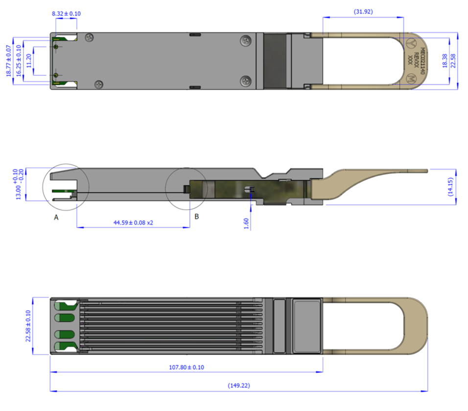
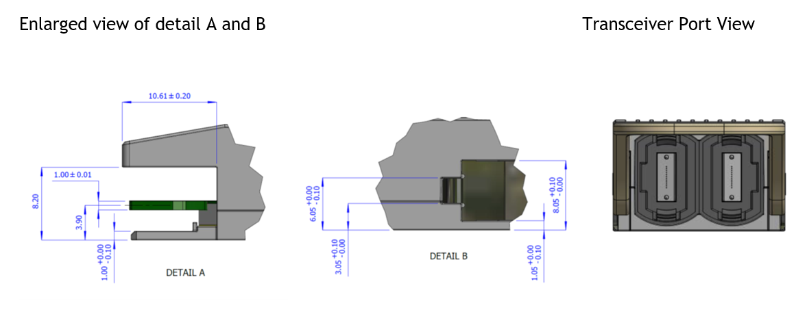
Finned-top twin-port for air-cooled 400G IB/EN Switches: Bottom, Side, and Top Views.
Option 1:
Option 2:
Option 3:
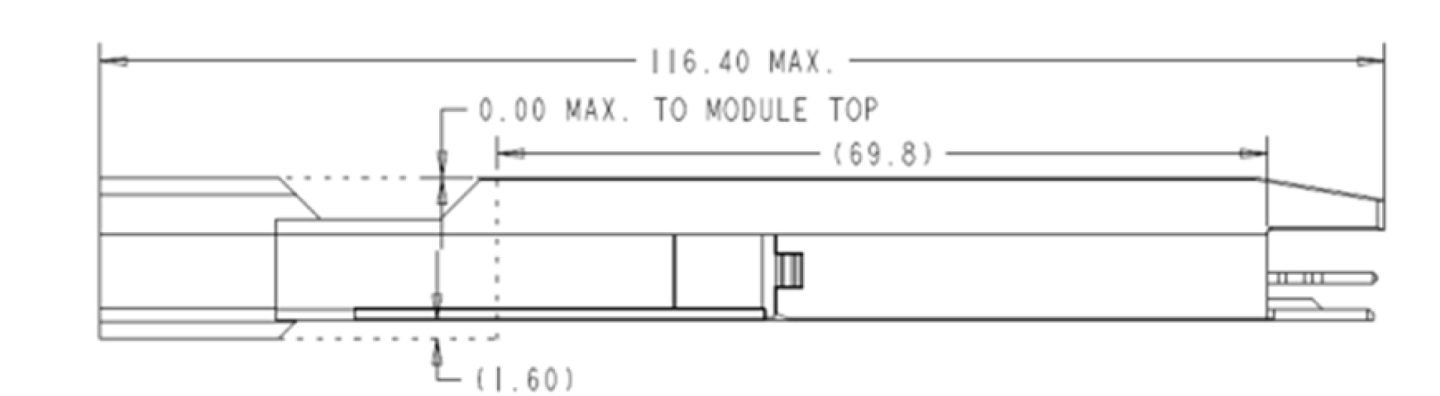
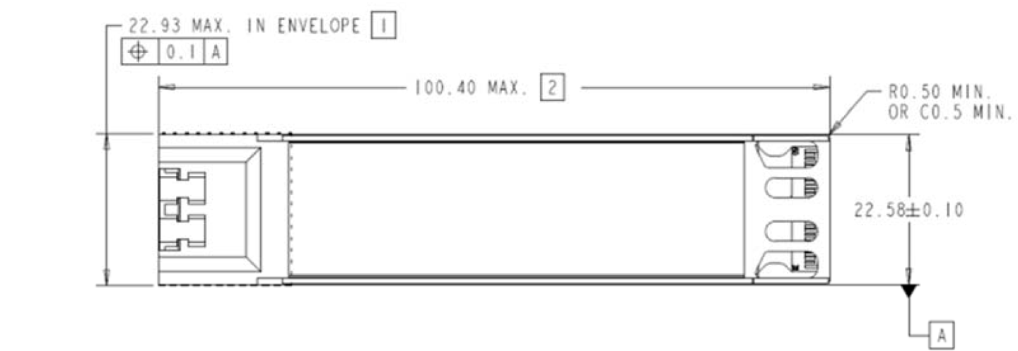
Front of the module. Pull tab and other components can extend 1.6mm max from the bottom of the module and can have up to 9.3mm width in the max envelope shown.
Applies to the type 1 module only.
Indicated surfaces (all 4 sides) to be conductive for connection to chassis ground.
Applies from the top of the module to the bottom of the module, Inside the cage.
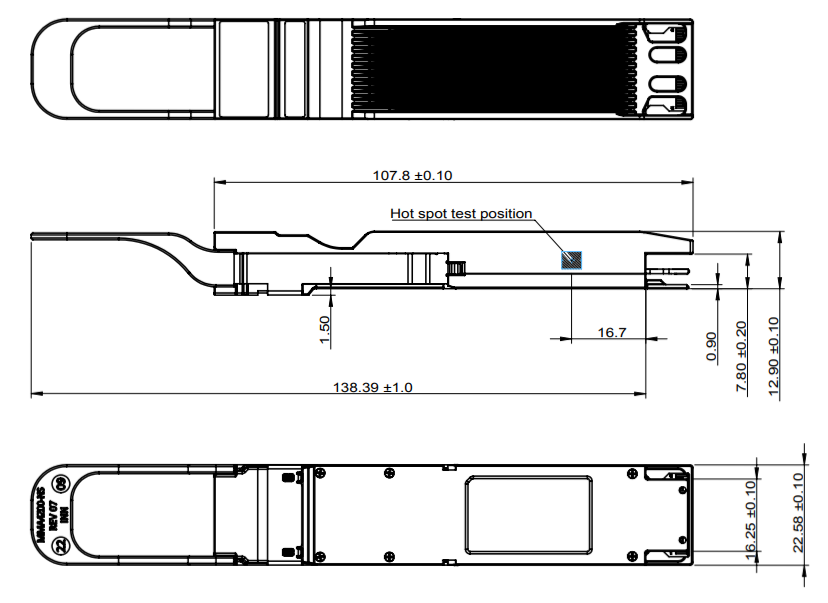
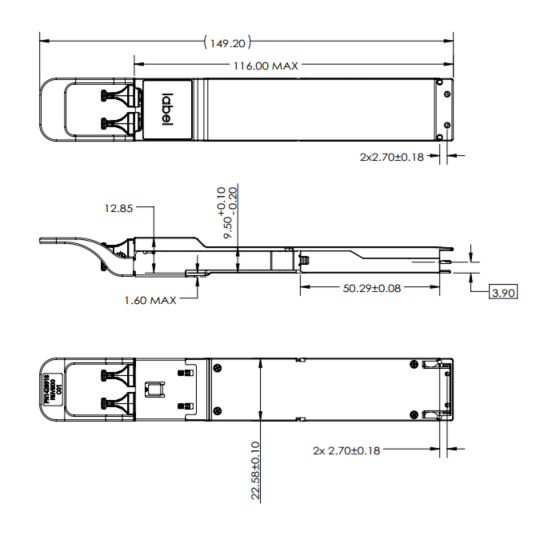
Flat-top Twin-port transceiver for DGX-H100 and Liquid-cooled Systems: Bottom, Side, and Top Views.
Transceiver Labeling and Fiber Polarity
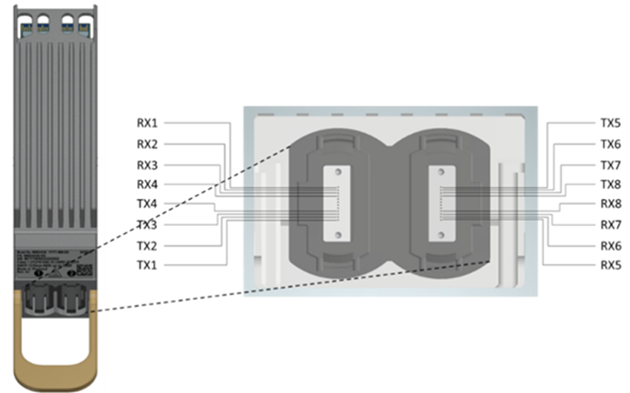
Transceiver port labeling and lane routing. Txn/Rxn refers to the OSFP pin description.
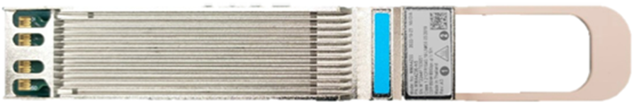
Tan pull-tab denotes multimode optics
Blue label denotes 50-meter reach
Back shell Label
The label applied on the transceiver's back-shell is illustrated below. Note that the Images are for illustration purposes only. Labels look and placement may vary.
Transceiver Label (Illustration)
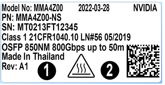
Images are for illustration purposes only. Product labels, colors, and form may vary.
Transceiver Back-Shell Label Serial Number Legend
|
Symbol |
Meaning |
Notes |
|
MT |
Manufacturer name (Mellanox Technologies) |
2 digits (alphanumeric) |
|
YY |
Year of manufacturing |
2 last digits of the year (numeric) |
|
WW |
Week of manufacturing |
2 digits (numeric) |
|
JC or DM |
Manufacturer Site: JC – Option 1 (China) DM – Option 2 (Malaysia) |
Two characters |
|
SSSSS |
Serial number |
5 digits (decimal numeric) for serial number, starting from 00001. |
Regulatory Compliance
The transceiver is a Class 1M laser product. It is certified per the following standards:
|
Feature |
Agency |
Standard |
|
Laser Eye Safety |
FDA/CDRH |
CDRH 21 CFR 1040 and Laser Notice 50 |
|
Electrical Safety |
CB |
IEC 62368 |
|
Electrical Safety |
UL/CSA |
UL 62368 and CAN/CSAN 62368 |

Warning: Exposure to the laser light can cause damage to the eyes. Use protective face gear while handling this product and keep the laser light away from the eyes and face.
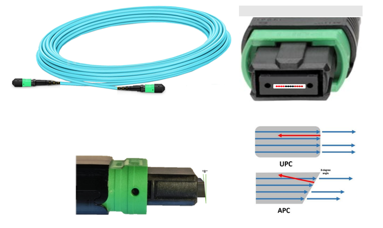
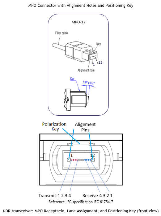
MPO-12/APC Optical Connector
The Twin-port NDR transceiver has a unique NVIDIA patented design enabling two, multiple-push-on/angled-polished-connector 12-fiber (MPO-12/APC) optical connectors per single OSFP form-factor by turning the optical connectors vertically in the twin-port transceiver end. This enables it to host two NDR transceivers inside, each with its own MPO-12/APC optical connector operating independently that can link to another Twin-port transceiver or to a single-port 400Gb/s NDR transceiver.
The MPO-12 has a 12-fiber ribbon but only 8-fibers are used – four transmit and four receive fibers for the 4-channels of 100G-PAM4 NDR.
The APC design minimizes back reflections and signal interference by diverting back reflected light from the fiber face to be absorbed into the fiber cladding.
A positioning key on top of the connector together with the alignment pins define the fiber position numbering scheme to align pin 1 in the optical connector to pin 1 in the transceiver also called “polarity”
Transceivers have alignment pins for precise positioning of the cable connector against the optical beams. The fiber cable has alignment holes matching the transceiver’s pins.
It is important to note that transceivers have pins. Optical connectors have holes and are used with transceivers. Optical connectors with pins are not compatible with transceivers and are used in trunk cabling to connect two fiber cables together.
The MPO-12/APC optical connector is used in both the NDR single mode and multimode fiber cables.
Multimode optics is denoted by a tan-colored pull tab and aqua-colored optical fiber. Green plastic shell on the MPO-12/APC connector denotes Angled Polish Connector and is not compatible with aqua colored shell for Ultra-flat Polished Connectors (UPC) for HDR.
MPO-12/APC Showing 4-Transmit and 4-Receive Fibers and Angled Polish Connector End
NVIDIA Supplied Crossover Type-B Fiber Cables
Linking two transceivers directly together requires aligning the transceiver laser sources with the correct photo detectors in the receive transceiver. Transmit and receive fibers are switched inside the cable enabling two transceivers to be directly connected to each other. This is called a Type-B crossover fiber.
Each of the two 4-channel NDR ports in the Twin-port transceiver has its own 4-channel optical connector that can link to two single-port 400Gb/s NDR transceiver. Two fiber cables are needed for each Twin-port transceiver.
Fiber cables are crossover cable Type-B that aligns the transmit laser with the opposite transceiver’s receiver photodetector allowing to directly connect two transceivers together to maintain minimum optical losses, lowest back reflections, longest reach and increased reliability without the use of optical patch panels. For Twin-port transceivers, both cables must be the same type (straight or 1:2 splitter) although different lengths are allowed.
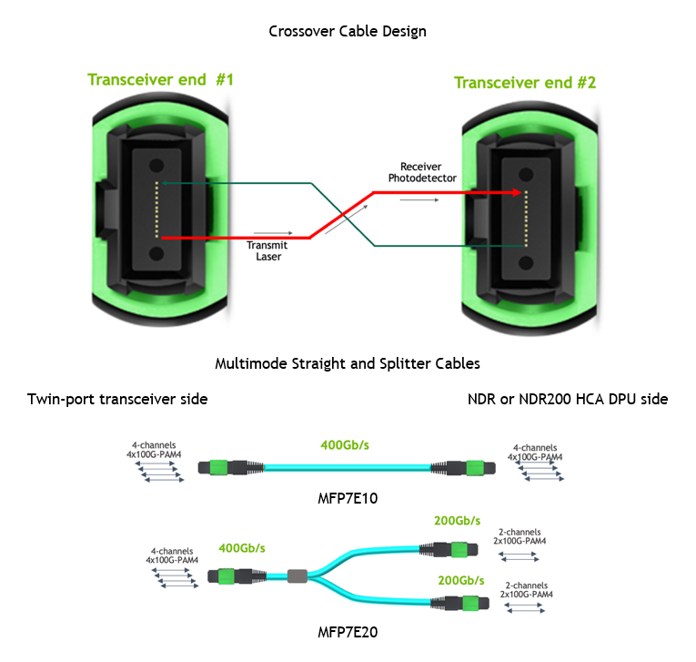
Note: Refer to the Recommended Fiber Cables table for more information.
Transceivers have alignment pins for precise positioning of the cable connector against the optical beams. The fiber cable has alignment holes matching the transceiver’s pins.
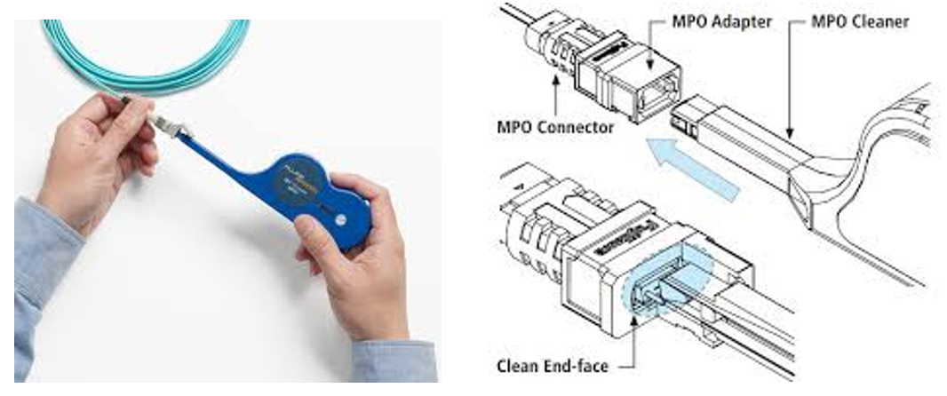
Handling and Cleaning
The transceiver can be damaged by exposure to current surges and over voltage events. Take care to restrict exposure to the conditions defined in Absolute Maximum Ratings. Observe normal handling precautions for electrostatic discharge-sensitive devices.
The transceiver is shipped with dust caps on both the electrical and the optical port. The cap on the optical port should always be in place when there is no fiber cable connected. The optical connector has a recessed connector surface which is exposed whenever it has no cable nor cap.
Important note 1: Keep both the fiber and transceiver dust caps.
Important note 2: Clean both transceiver receptacle and cable connector prior to insertion of the fiber cable, to prevent contamination from it.
The dust cap ensures that the optics remain clean during transportation. Standard cleaning tools and methods should be used during installation and service. Liquids must not be applied.
Important note 3: 80% of transceiver link problems are related to dirty optical connectors.
Cable Management Guidelines
For more information and general interconnect management and installation, see NVIDIA Cable Management Guidelines and FAQ Application Note.