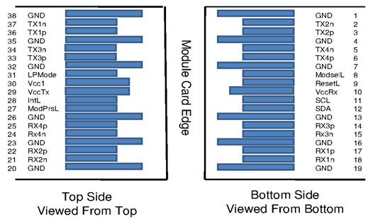
Pin Descriptions
Pin | Symbol | Description | Pin | Symbol | Description |
1 | GND | Ground | 20 | GND | Ground |
2 | Tx2n | Transmitter Inverted Data Input | 21 | Rx2n | Receiver Inverted Data Output |
3 | Tx2p | Transmitter Non-Inverted Data Input | 22 | Rx2p | Receiver Non-Inverted Data Output |
4 | GND | Ground | 23 | GND | Grounds |
5 | Tx4n | Transmitter Inverted Data Input | 24 | Rx4n | Receiver Inverted Data Output |
6 | Tx4p | Transmitter Non-Inverted Data Input | 25 | Rx4p | Receiver Non-Inverted Data |
7 | GND | Ground | 26 | GND | Ground |
8 | ModSelL | Module Select | 27 | ModPrsL | Module Present |
9 | ResetL | Module Reset | 28 | IntL | Interrupt |
10 | Vcc Rx | +3.3V Power Supply Receiver | 29 | Vcc Tx | +3.3V Power Supply Transmitter |
11 | SCL | 2-wire Serial Interface Clock | 30 | Vcc1 | +3.3V Power Supply |
12 | SDA | 2-wire Serial Interface Data | 31 | LPMode | Low Power Mode |
13 | GND | GND | 32 | GND | Ground |
14 | Rx3p | Receiver Non-Inverted Data Output | 33 | Tx3p | Transmitter Non-Inverted Data Input |
15 | Rx3n | Receiver Inverted Data Output | 34 | Tx3n | Transmitter Inverted Data Input |
16 | GND | Ground | 35 | GND | Ground |
17 | Rx1p | Receiver Non-Inverted Data Output | 36 | Tx1p | Transmitter Non-Inverted Data Input |
18 | Rx1n | Receiver Inverted Data Output | 37 | Tx1n | Transmitter Inverted Data Input |
19 | GND | Ground | 38 | GND | Ground |
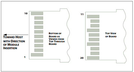
QSFP28 Module Pad Layout
The MCP7F00 DAC is compatible with ESD levels in typical data center operating environments and certified in accordance with the standards listed in the Regulatory Compliance section. The product is shipped with protective caps on its connectors to protect it until the time of installation. In normal handling and operation of high-speed cables and optical transceivers, ESD is of concern during insertion into the QSFP cage of the server/switch. Hence, standard ESD handling precautions must be observed. These include use of grounded wrist/shoe straps and ESD floor wherever a cable/transceiver is extracted/inserted. Electrostatic discharges to the exterior of the host equipment chassis after installation are subject to system level ESD requirements.
Pin | Connector Pin Name | Port A Signal Name |
1 | VeeT | Module Transmitter Ground |
2 | Tx_Fault | Module Transmitter Fault |
3 | Tx_Disable | Transmitter Disable. Turns off transmitter laser output |
4 | SDA | 2-wire Serial Interface Data Line |
5 | SCL | 2-wire Serial Interface Clock |
6 | Mod_ABS | Module Absent. Grounded within the module |
7 | RS0 | Rate Select 0, optionally controls SFP+ module receiver |
8 | Rx_LOS | Receiver Loss of Signal Indication |
9 | RS1 | Rate Select 1, optionally controls SFP+ module transmitter |
10 | VeeR | Module Receiver Ground |
11 | VeeR | Module Receiver Ground |
12 | RD- | Receiver Inverted Data Output |
13 | RD+ | Receiver Non-Inverted Data Output |
14 | VeeR | Module Receiver Ground |
15 | VccR | Module Receiver Power Supply |
16 | VccT | Module Transmitter Power Supply |
17 | VeeT | Module Transmitter Ground |
18 | TD+ | Transmitter Non-Inverted Data Input. AC coupled |
19 | TD- | Transmitter Inverted Data Input. AC coupled |
20 | VeeT | Module Transmitter Ground |
SFP28 Module Pad Layout