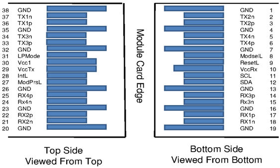
Pin Description
The QSFP28 pin assignment is SFF-8679 compliant.
Pin | Symbol | Description | Pin | Symbol | Description |
1 | Ground | Ground | 20 | Ground | Ground |
2 | Tx2n | Connected to Port 1 lane Rx2 | 21 | Rx2n | Connected to Port 1 lane Tx2 |
3 | Tx2p | Connected to Port 1 lane Rx2 | 22 | Rx2p | Connected to Port 1 lane Tx2 |
4 | Ground | Ground | 23 | Ground | Grounds |
5 | Tx4n | Connected to Port 2 lane Rx2 | 24 | Rx4n | Connected to Port 2 lane Tx2 |
6 | Tx4p | Connected to Port 2 lane Rx2 | 25 | Rx4p | Connected to Port 2 lane Tx2 |
7 | Ground | Ground | 26 | Ground | Ground |
8 | Mod-SelL | Cable Select | 27 | ModPrsL | Cable Present |
9 | ResetL | Cable Reset | 28 | IntL | Interrupt |
10 | Vcc Rx | +3.3V Power supply receiver | 29 | Vcc Tx | +3.3V Power supply transmitter |
11 | SCL | 2-wire serial interface clock | 30 | Vcc1 | +3.3V Power Supply |
12 | SDA | 2-wire serial interface data | 31 | LPMode | Low Power Mode |
13 | Ground | Ground | 32 | Ground | Ground |
14 | Rx3p | Connected to Port 2 lane Tx1 | 33 | Tx3p | Connected to Port 2 lane Rx1 Non-Inverted Data |
15 | Rx3n | Connected to Port 2 lane Tx1 | 34 | Tx3n | Connected to Port 2 lane Rx1 |
16 | Ground | Ground | 35 | Ground | Ground |
17 | Rx1p | Connected to Port 1 lane Tx1 | 36 | Tx1p | Connected to Port 1 lane Rx1 |
18 | Rx1n | Connected to Port 1 lane Tx1 | 37 | Tx1n | Connected to Port 1 lane Rx1 |
19 | Ground | Ground | 38 | Ground | Ground |
QSFP28 Module Pad Layout
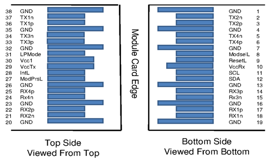
Pin | Symbol | Description | Pin | Symbol | Description |
1 | Ground | Ground | 20 | Ground | Ground |
2 | Tx2n | Connected to lane Rx2 | 21 | Rx2n | Connected to lane Tx2 |
3 | Tx2p | Connected to lane Rx2 | 22 | Rx2p | Connected to lane Tx2 |
4 | Ground | Ground | 23 | Ground | Grounds |
5 | Not connected | Not connected | 24 | Not connected | Not connected |
6 | Not connected | Not connected | 25 | Not connected | Not connected |
7 | Ground | Ground | 26 | Ground | Ground |
8 | Mod-SelL | Cable Select | 27 | ModPrsL | Cable Present |
9 | ResetL | Cable Reset | 28 | IntL | Interrupt |
10 | Vcc Rx | +3.3V Power supply receiver | 29 | Vcc Tx | +3.3V Power supply transmitter |
11 | SCL | 2-wire serial interface clock | 30 | Vcc1 | +3.3V Power Supply |
12 | SDA | 2-wire serial interface data | 31 | LPMode | Low Power Mode |
13 | Ground | Ground | 32 | Ground | Ground |
14 | Not connected | Not connected | 33 | Not connected | Not connected |
15 | Not connected | Not connected | 34 | Not connected | Not connected |
16 | Ground | Ground | 35 | Ground | Ground |
17 | Rx1p | Connected to lane Tx1 | 36 | Tx1p | Connected to lane Rx1 |
18 | Rx1n | Connected to lane Tx1 | 37 | Tx1n | Connected to lane Rx1 |
19 | Ground | Ground | 38 | Ground | Ground |
QSFP28 Module Pad Layout
The pinout of the 50Gb/s ends of the cable is identical to the 100Gb/s end except that RF lanes 3 and 4 (pins 5, 6, 14, 15, 24, 25, 33, 34) are not connected.