Pin Descriptions
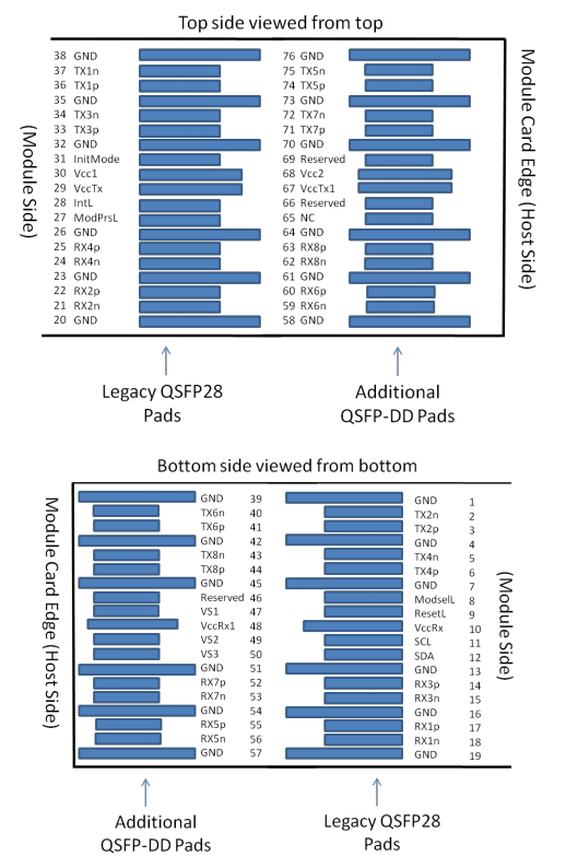
The head end of the MCP7H60 cable has the pad assignment shown below, which is compliant with the QSFP-DD Hardware Specification [2].
|
Pin |
Symbol |
Description |
Pin |
Symbol |
Description |
|
1 |
GND |
Ground |
39 |
GND |
Ground |
|
2 |
Tx2n |
Transmitter Inverted Data Input |
40 |
Tx6n |
Transmitter Inverted Data Input |
|
3 |
Tx2p |
Transmitter Non-Inverted Data Input |
41 |
Tx6p |
Transmitter Non-Inverted Data Input |
|
4 |
GND |
Ground |
42 |
GND |
Ground |
|
5 |
Tx4n |
Transmitter Inverted Data Input |
43 |
Tx8n |
Transmitter Inverted Data Input |
|
6 |
Tx4p |
Transmitter Non-Inverted Data Input |
44 |
Tx8p |
Transmitter Non-Inverted Data Input |
|
7 |
GND |
Ground |
45 |
GND |
Ground |
|
8 |
ModSelL |
Module Select |
46 |
Reserved |
|
|
9 |
ResetL |
Module Reset |
47 |
VS1 |
Module Vendor Specific 1 |
|
10 |
VccRx |
+3.3V Power Supply Receiver |
48 |
VccRx1 |
+3.3V Power Supply Receiver |
|
11 |
SCL |
2-wire Serial Interface Clock |
49 |
VS2 |
Module Vendor Specific 2 |
|
12 |
SDA |
2-wire Serial Interface Data |
50 |
VS3 |
Module Vendor Specific 3 |
|
13 |
GND |
GND |
51 |
GND |
Ground |
|
14 |
Rx3p |
Receiver Non-Inverted Data Output |
52 |
Rx7p |
Receiver Non-Inverted Data Output |
|
15 |
Rx3n |
Receiver Inverted Data Output |
53 |
Rx7n |
Receiver Inverted Data Output |
|
16 |
GND |
Ground |
54 |
GND |
Ground |
|
17 |
Rx1p |
Receiver Non-Inverted Data Output |
55 |
Rx5p |
Receiver Non-Inverted Data Output |
|
18 |
Rx1n |
Receiver Inverted Data Output |
56 |
Rx5n |
Receiver Inverted Data Output |
|
19 |
GND |
Ground |
57 |
GND |
Ground |
|
20 |
GND |
Ground |
58 |
GND |
Ground |
|
21 |
Rx2n |
Receiver Inverted Data Output |
59 |
Rx6n |
Receiver Inverted Data Output |
|
22 |
Rx2p |
Receiver Non-Inverted Data Output |
60 |
Rx6p |
Receiver Non-Inverted Data Output |
|
23 |
GND |
Ground |
61 |
GND |
Grounds |
|
24 |
Rx4n |
Receiver Inverted Data Output |
62 |
Rx8n |
Receiver Inverted Data Output |
|
25 |
Rx4p |
Receiver Non-Inverted Data Output |
63 |
Rx8p |
Receiver Non-Inverted Data Output |
|
26 |
GND |
Ground |
64 |
GND |
Ground |
|
27 |
ModPrsL |
Module Present |
65 |
NC |
|
|
28 |
IntL |
Interrupt |
66 |
Reserved |
|
|
29 |
VccTx |
+3.3V Power Supply Transmitter |
67 |
VccTx1 |
+3.3V Power Supply Transmitter |
|
30 |
Vcc1 |
+3.3V Power Supply |
68 |
Vcc2 |
+3.3V Power Supply |
|
31 |
LPMode |
Low Power Mode |
69 |
Reserved |
|
|
32 |
GND |
Ground |
70 |
GND |
Ground |
|
33 |
Tx3p |
Transmitter Non-Inverted Data Input |
71 |
Tx7p |
Transmitter Non-Inverted Data Input |
|
34 |
Tx3n |
Transmitter Inverted Data Input |
72 |
Tx7n |
Transmitter Inverted Data Input |
|
35 |
GND |
Ground |
73 |
GND |
Ground |
|
36 |
Tx1p |
Transmitter Non-Inverted Data Input |
74 |
Tx5p |
Transmitter Non-Inverted Data Input |
|
37 |
Tx1n |
Transmitter Inverted Data Input |
75 |
Tx5n |
Transmitter Inverted Data Input |
|
38 |
GND |
Ground |
76 |
GND |
Ground |
QSFP-DD Module Pad Layout
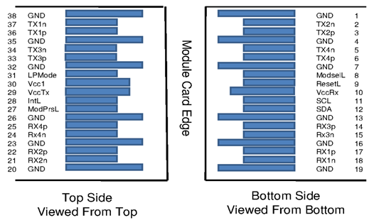
The 200G ‘tails’ of the MCP7H60 cable are compliant with the QSFP specifications SFF-8665, etc. [3][4][5]. The connectors have the pin assignment shown below.
|
Pin |
Symbol |
Description |
Pin |
Symbol |
Description |
|
1 |
GND |
Ground |
20 |
GND |
Ground |
|
2 |
Tx2n |
Transmitter Inverted Data Input |
21 |
Rx2n |
Receiver Inverted Data Output |
|
3 |
Tx2p |
Transmitter Non-Inverted Data Input |
22 |
Rx2p |
Receiver Non-Inverted Data Output |
|
4 |
GND |
Ground |
23 |
GND |
Grounds |
|
5 |
Tx4n |
Transmitter Inverted Data Input |
24 |
Rx4n |
Receiver Inverted Data Output |
|
6 |
Tx4p |
Transmitter Non-Inverted Data Input |
25 |
Rx4p |
Receiver Non-Inverted Data Output |
|
7 |
GND |
Ground |
26 |
GND |
Ground |
|
8 |
ModSelL |
Module Select |
27 |
ModPrsL |
Module Present |
|
9 |
ResetL |
Module Reset |
28 |
IntL |
Interrupt |
|
10 |
Vcc Rx |
+3.3V Power Supply Receiver |
29 |
Vcc Tx |
+3.3V Power Supply Transmitter |
|
11 |
SCL |
2-wire Serial Interface Clock |
30 |
Vcc1 |
+3.3V Power Supply |
|
12 |
SDA |
2-wire Serial Interface Data |
31 |
LPMode |
Low Power Mode |
|
13 |
GND |
GND |
32 |
GND |
Ground |
|
14 |
Rx3p |
Receiver Non-Inverted Data Output |
33 |
Tx3p |
Transmitter Non-Inverted Data Input |
|
15 |
Rx3n |
Receiver Inverted Data Output |
34 |
Tx3n |
Transmitter Inverted Data Input |
|
16 |
GND |
Ground |
35 |
GND |
Ground |
|
17 |
Rx1p |
Receiver Non-Inverted Data Output |
36 |
Tx1p |
Transmitter Non-Inverted Data Input |
|
18 |
Rx1n |
Receiver Inverted Data Output |
37 |
Tx1n |
Transmitter Inverted Data Input |
|
19 |
GND |
Ground |
38 |
GND |
Ground |
QSFP56 Module Pad Layout
This head end of the MCP7H60 is QSFP-Double Density and QSFP56 and the ‘tails’ are QSFP56. This means that the control signals shown in the pad layout and the pin assignments have the following functions:
|
Name |
Function |
Description |
|
ModPrsL |
Output, asserted low |
Pull-up by host when no cable is present. The cable is connecting the signal to ground. Hence, asserted when the cable is plugged in. |
|
ModSelL |
Input, asserted low |
Asserted by host to activate the I2C (two-wire interface) to the EEPROM inside the cable. |
|
ResetL |
Input, asserted low |
Must be de-asserted to enable the host system to read the EEPROM. |
|
LPMode |
Input, asserted high |
Not connected in DAC cables. |
|
ePPS |
Input |
Not connected in DAC cables |
|
IntL |
Output, asserted low |
Not used in DAC cables, internally pulled high. |