Specifications
Absolute maximum ratings are those beyond which damage to the device may occur.
Prolonged operation between the operational specifications and absolute maximum ratings is not intended and may cause permanent device degradation.
Parameter | Min | Max | Units | |
Supply voltage | -0.3 | 3.6 | V | |
Data input voltage | -0.3 | 3.465 | V | |
Control input voltage | -0.3 | 4 | V | |
Damage threshold (a) | 3.4 | --- | dBm | |
This table shows the environmental specifications for the product.
Parameter | Min | Max | Units |
Storage temperature | -40 | 85 | °C |
This section shows the range of values for normal operation.
Parameter | Min | Typ | Max | Units |
Supply voltage | 3.135 | 3.3 | 3.465 | V |
Power dissipation | --- | 1.3 | 1.5 | W |
Supply noise tolerance (10 Hz – 10 MHz) | 66 | --- | --- | mVpp |
Operating case temperature | 0 | --- | 70 | °C |
Operating relative humidity | 5 | --- | 85 | %RH |
Parameter (per lane) | Min | Typ | Max | Units |
Signaling rate | -100ppm | 14.0625 | +100ppm | Gb/s |
Differential data input swing at TP1a | 100 | --- | 900 | mVpp |
Differential data output swing at TP4 | 300 | --- | 600 | mVpp |
J2 jitter tolerance (TP6) | --- | --- | 0.19 | UI |
J9 jitter tolerance (TP6) | --- | --- | 0.34 | UI |
Data dependent pulse width shrinkage (DDPWS) | --- | --- | 0.07 | UI |
Output Transition time, 20 to 80% | 20 | --- | --- | Ps |
J2 jitter output (TP7) | --- | --- | 0.44 | UI |
J9 jitter output (TP7) | --- | --- | 0.69 | UI |
Note 1: Requires optimization of the input equalizer.
Parameter | Min | Typ | Max | Units |
Transmitter (per lane) | ||||
Signaling Speed | 100ppm | 14.0625 | +100ppm | Gb/s |
Center Wavelength | 840 | --- | 860 | nm |
Average Launch Power | -7.6 | --- | 2.4 | dBm |
Transmit OMA | -5.6 | --- | 3 | dBm |
Extinction Ratio | 3 | --- | --- | dB |
Average Launch power at Tx squelched | --- | --- | -30 | dBm |
Eye Crossing | 45 | --- | 55 | % |
Optical return loss tolerance | --- | --- | 12 | dB |
Reach on OM3 Multi-mode fiber | --- | --- | 30 | m |
Receiver (per lane) | ||||
Signaling Speed | 100ppm | 14.0625 | +100ppm | Gb/s |
Center Wavelength | 840 | --- | 860 | nm |
Receiver Reflectance | --- | --- | -12 | dB |
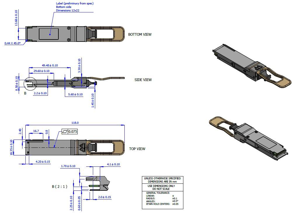
Mechanical Dimensions
The following label is applied on the transceiver's backshell:
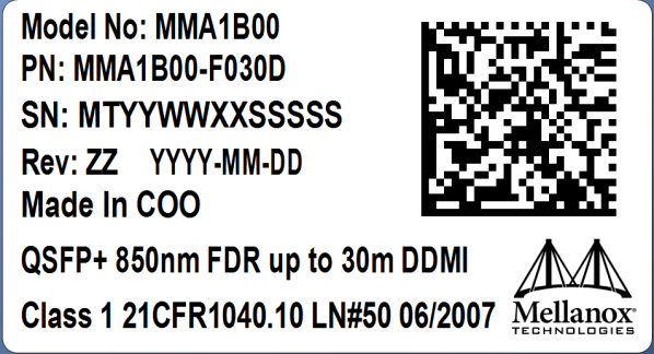
(sample illustration)
Backshell Label SN (Serial Number) Legend
Symbol | Meaning | Notes | |
SN – Serial Number | |||
MT | Manufacturer name | 2 characters, e.g. MT | |
YY | Year of manufacturing | 2 digits | |
WW | Week of manufacturing | 2 digits | |
XX | Manufacturer site | 2 characters | |
SSSSS | Serial number | 5 digits for serial number, starting from 00001. Reset at start of week to 00001. | |
Miscellaneous | |||
ZZ | HW and SW revision | 2 alpha-numeric characters | |
YYYY | Year of manufacturing | 4 digits | |
MM | Month of manufacturing | 2 digits | |
DD | Day of manufacturing | 2 digits | |
COO | Country of origin | E.g. China or Malaysia | |

| Quick response code | Serial number (MTYYWWXXSSSSS) | |
Regulatory Compliance and Classification
The laser module is classified as Class 1 according to IEC 60825-1, IEC 60825-2 and 21 CFR sub J 1040 (CDRH), TÜV/UL60950-1, CAN/CSA-C22.2 60950-1.
EMC: EN55032 Class A, EN55024, AS/NZS CISPR 32 Class A, CISPR32 Class A, VCCI Class A.
Telcordia Technologies© GR-468CORE, (shock, vibration, HT operation, damp heat operation).
Ask your field engineer or Mellanox support for a zip file of the certifications for this product.
This device complies with CFR47 FCC Class A Part 15 of the FCC Rules. Operation is subject to the following two conditions:
This device may not cause harmful interference.
This device must accept any interference received, including interference that may cause undesired operation.
Note: This equipment has been tested and found to comply with the limits for a Class A digital device, pursuant to Part 15 of the FCC Rules. These limits are designed to provide reasonable protection against harmful interference in a residential installation. This equipment generates, uses and can radiate radio frequency energy and, if not installed and used in accordance with the instructions, may cause harmful interference to radio communications. However, there is no guarantee that interference will not occur in a particular installation. If this equipment does cause harmful interference to radio or television reception, which can be determined by turning the equipment off and on, the user is encouraged to try to correct the interference by one or more of the following measures:
Reorient or relocate the receiving antenna.
Increase the separation between the equipment and receiver.
Connect the equipment into an outlet on a circuit different from that to which the receiver is connected.
Consult the dealer or an experienced radio/television technician for help.
Modifications: Any modifications made to this device that are not approved by NVIDIA may void the authority granted to the user by the FCC to operate this equipment.