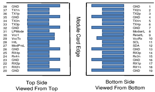
Pin Description
The transceiver’s pin assignment is SFF-8679 compliant.
Pin | Symbol | Description | Pin | Symbol | Description |
1 | GND | Ground | 20 | GND | Ground |
2 | Tx2n | Transmitter Inverted Data Input | 21 | Rx2n | Receiver Inverted Data Output |
3 | Tx2p | Transmitter Non-Inverted Data Input | 22 | Rx2p | Receiver Non-Inverted Data Output |
4 | GND | Ground | 23 | GND | Grounds |
5 | Tx4n | Transmitter Inverted Data Input | 24 | Rx4n | Receiver Inverted Data Output |
6 | Tx4p | Transmitter Non-Inverted Data Input | 25 | Rx4p | Receiver Non-Inverted Data Output |
7 | GND | Ground | 26 | GND | Ground |
8 | ModSelL | Module Select | 27 | ModPrsL | Module Present |
9 | ResetL | Module Reset | 28 | IntL | Interrupt |
10 | Vcc Rx | +3.3V Power Supply Receiver | 29 | Vcc Tx | +3.3V Power Supply Transmitter |
11 | SCL | 2-wire Serial Interface Clock | 30 | Vcc1 | +3.3V Power Supply |
12 | SDA | 2-wire Serial Interface Data | 31 | LPMode | Low Power Mode |
13 | GND | GND | 32 | GND | Ground |
14 | Rx3p | Receiver Non-Inverted Data Output | 33 | Tx3p | Transmitter Non-Inverted Data Input |
15 | Rx3n | Receiver Inverted Data Output | 34 | Tx3n | Transmitter Inverted Data Input |
16 | GND | Ground | 35 | GND | Ground |
17 | Rx1p | Receiver Non-Inverted Data Output | 36 | Tx1p | Transmitter Non-Inverted Data Input |
18 | Rx1n | Receiver Inverted Data Output | 37 | Tx1n | Transmitter Inverted Data Input |
19 | GND | Ground | 38 | GND | Ground |
Notes:
GND is the symbol for signal and supply (power) common for the QSFP28 module. All are common within the module and all module voltages are referenced to this potential unless otherwise noted. Connect these directly to the host board signal common ground plane.
VccRx, Vcc1 and VccTx are the receiving and transmission power suppliers and shall be applied concurrently.
Vcc Rx, Vcc1 and Vcc Tx may be internally connected within the module in any combination. The connector pins are each rated for a maximum current of 1000 mA.
QSFP28 Module Pad Layout
This transceiver is SFF-8636 compliant. This means that the control signals shown in the pad layout support the following functions:
Name | Function | Description |
ModPrsL | Output, asserted low | Module Present pin, grounded inside the module. Terminated with pull-up in the host system. Asserted low when the transceiver is inserted, whereby the host detects the presence of the transceiver. |
ModSelL | Input, asserted Low | Module Select input pin, terminated high in the module. Only when held low by the host, the module responds to 2-wire serial communication commands. The ModSelL enables multiple modules to share a single 2-wire interface bus. |
ResetL | Input, asserted Low | Reset input pin, pulled high in the module. A low level on the ResetL pin for longer than the minimum pulse length (t_Reset_init) initiates a complete module reset, returning all user module settings to their default state. During reset the host shall disregard all status bits until the module indicates completion of the reset interrupt by asserting IntL signal low with the Data_Not_Ready bit negated. |
LPMode | Input, asserted high | Low Power Mode input, pulled up inside the module. The transceiver starts up in low-power mode, i.e. <1.5 W with the two-wire interface active. The host system can read the power class declaration from the transceiver and determine if it has enough power to enable the high-speed operation/high power mode of the transceiver. This can be done by asserting LPMode low or by use of the Power_over-ride and Power_set control bits (Address A0h, byte 93 bits 0,1). |
IntL | Output, asserted low | Interrupt Low is an open-collector output, terminated high in the host system. A “Low” indicates a possible module operational fault or a status critical to the host system, e.g. temperature alarm. The host identifies the source of the interrupt using the 2-wire serial interface. The INTL pin is de-asserted “High” after completion of reset, when byte 2 bit 0 (Data Not Ready) is read with a value of ‘0’. |
The low-speed signals are Low Voltage TTL (LVTTL) compliant (except for SCL and SDA signals).
The transceiver complies with the SFF-8665 specification and has the following key features:
Physical layer link optimization:
Programmable Tx input equalization
Programmable Rx output amplitude
Programmable Rx output pre-emphasis
Tx/Rx CDR control
by default enabled for 100 GbE operation, disable it for 40G operation
Digital Diagnostic Monitoring (DDM):
Rx receive optical power monitor for each lane
Tx transmit optical power monitor for each lane
Tx bias current monitor for each lane
Supply voltage monitor
Transceiver case temperature monitor
Warning and Alarm thresholds for each DDM function (not user changeable)
Other SFF-8636 functions and interrupt indications:
Tx & Rx LOS indication
Tx & Rx LOL indication
Tx fault indication
LOS, LOL, and Tx Fault status flags can be read via the two-wire management interface and are jointly transmitted via the IntL output pin. Relevant advertisement, threshold, and readout registers are found in the SFF-8636 MSA.