Specifications
Absolute maximum ratings are those beyond which permanent damage to the device may occur.
Parameter | Symbol | Min | Max | Units |
Storage Temperature | TS | -40 | 85 | °C |
Operating Case Temperature | TOP | 0 | 70 | °C |
Maximum Supply Voltage | Vcc | -0.5 | 3.6 | V |
Relative Humidity (non-condensing) | RH – Option 1 | 5 | 95 | % |
RH – Option 2 | 15 | 85 | % | |
Control Input Voltage | VI | -0.3 | Vcc+0.5 | V |
IO | -20 | 20 | mA |
Parameter | Symbol | Min | Typ | Max | Units |
Supply Voltage | VccRx, Vcc1, VccTx | 3.135 | --- | 3.465 | V |
Data Rate, each Lane | --- | -100 ppm | 25.78125 | + 100 ppm | Gbps |
Control Input Voltage High | VIH | VCC*0.7 | --- | VCC+0.3 | V |
Control Input Voltage Low | VIL | -0.3 | --- | VCC*0.3 | V |
Power Supply Noise Tolerance (10Hz -10MHz) | 66 | mVpp | |||
Rx Differential Data Output Load | 100 | Ω | |||
Link Distance with G.652 compliant fiber | Lmax | 2 | --- | 2000 | m |
Parameter | Symbol | Min | Typical | Max | Units | Notes | |
Power Consumption | PD | --- | --- | 3.5 | W | ||
Transmitter (each lane) | |||||||
Differential Data Input Amplitude | VIN,PP | 95 | --- | 900 | mVpp | 1 | |
Differential termination mismatch | 10 | % | |||||
LPMode, Reset and ModSelL | VIL | -0.3 | --- | VCC*0.3 | V | ||
VIH | VCC*0.7 | --- | VCC+0.3 | ||||
Receiver (each lane) | |||||||
Differential Data Output Amplitude | VOUT,PP | 250 | --- | 900 | mVpp | 1 | |
Differential termination mismatch | --- | --- | 10 | % | |||
Output Rise/Fall Time, 20% to 80% | tr | 9.5 | --- | --- | ps | ||
ModPrsL and IntL | VOL | 0 | --- | 0.4 | V | IOL=4mA | |
VOH | VCC-0.5 | --- | VCC+0.3 | V | |||
Notes:
Amplitude customization beyond these specs is dependent on validation in customer system.
Parameter | Symbol | Min | Typical | Max | Units | Notes |
Signaling Speed per Lane | 25.78125 ± 100 ppm | Gb/s | 1 | |||
Lane Wavelength | L0 | 1294.53 | --- | 1296.59 | nm | |
L1 | 1299.02 | --- | 1301.09 | nm | ||
L2 | 1303.54 | --- | 1305.63 | nm | ||
L3 | 1308.09 | --- | 1310.19 | nm | ||
Transmitter | ||||||
Sidemode Suppression Ratio (SMSR) | SMSR | 30 | --- | --- | dB | |
Total Average Launch Power | PT | --- | --- | 10.5 | dBm | |
Average Launch Power, each Lane | PAVG | -4.3 | 4.5 | dBm | 2, 7 | |
Optical Modulation Amplitude (OMA), each Lane | POMA | -1.3 | --- | 4.5 | dBm | |
Extinction Ratio | ER | 4 | --- | --- | dB | |
Relative Intensity Noise (RIN) | RIN | --- | --- | -130 | dB/Hz | |
Optical Return Loss Tolerance | ORLT | --- | --- | 20 | dB | |
Transmitter Reflectance | RT | --- | --- | -12 | dB | |
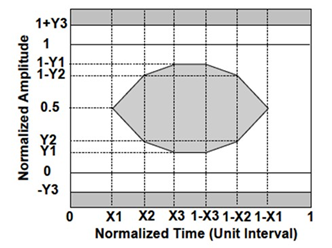
Eye Mask {X1, X2, X3, Y1, Y2, Y3} | {0.25, 0.4, 0.45, 0.25, 0.28, 0.4} | 3 | ||||
Average Launch Power OFF Transmitter, each Lane | POFF | --- | --- | -30 | dBm | |
Receiver | ||||||
Signaling Speed per Lane | 25.78125 ± 100 ppm | GBd | 4 | |||
Receive Power (OMA), each Lane | --- | --- | --- | 4.5 | dBm | |
Average Receive Power per Lane | RXPx | -10.6 | --- | 4.5 | dBm | 5, 7 |
Receiver Sensitivity (OMA), each Lane | SEN | --- | --- | -8.6 | dBm | |
Stressed Receiver Sensitivity (OMA), each Lane | --- | --- | -6.8 | dBm | 6 | |
LOS De-Assert | LOSD | --- | --- | -11.6 | dBm | |
LOS Assert | LOSA | --- | --- | -13.6 | dBm | |
LOS Hysteresis | LOSH | --- | 1.5 | --- | dBm | |
Notes:
Transmitter consists of 4 lasers operating at 25.78Gb/s each.
Minimum value is informative.
Hit ratio 5x10⁻⁵.
Minimum value is informative, equals min Tx OMA with infinite ER and max channel insertion loss.
SRS is measured with vertical eye closure penalty of 1.8 dB max, J2 of 0.30 UI, and J9 of 0.47 UI.
Power value and power accuracy are with all channels enabled.
Eye Mask Definition
This product is compatible with ESD levels in typical data center operating environments and certified in accordance with the standards listed in the Regulatory Compliance Section. The product is shipped with protective caps on all connectors to protect it during shipping. In normal handling and operation of high-speed cables and optical transceivers, ESD is of concern during insertion into the OSFP cage of the server/switch. Hence, standard ESD handling precautions must be observed. These include use of grounded wrist/shoe straps and ESD floor wherever a cable/transceiver is extracted/inserted. Electrostatic discharges to the exterior of the host equipment chassis after installation are subject to system level ESD requirements.
The transceiver can be damaged by exposure to current surges and over voltage events. Take care to restrict exposure to the conditions defined in Absolute Maximum Ratings. Observe normal handling precautions for electrostatic discharge-sensitive devices. The transceiver is shipped with dust caps on both the electrical and the optical port. The cap on the optical port should always be in place when there is no fiber cable connected. The optical connector has a recessed connector surface which is exposed whenever it has no cable nor cap.
Prior to insertion of the fiber cable, clean the cable connector to prevent contamination from it. The dust cap ensures that the optics remain clean and no additional cleaning should be needed. In the event of contamination, standard cleaning tools and methods should be used. Liquids must not be applied.
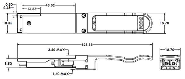
Mechanical Dimensions
The transceiver’s memory map is compliant with the QSFP Management interface specification SFF-8636. See also the NVIDIA LinkX® Memory Map Application Note (MLNX-15-5926).
The following label is applied on the transceiver's backshell:
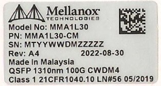
(sample illustration)
Backshell Label Legend
Symbol | Meaning | Notes |
SN – Serial Number | ||
MT | Manufacturer name | 2 characters (MT) |
YY | Year of manufacturing | 2 digits |
WW | Week of manufacturing | 2 digits |
DM | Manufacturer site | 2 characters |
ZZZZZ | Serial number | 5 digits for serial number, starting from 00001. Reset at start of week to 00001. |
Miscellaneous | ||
ZZ | HW and SW revision | 2 alpha-numeric characters |
YYYY | Year of manufacturing | 4 digits |
MM | Month of manufacturing | 2 digits |
DD | Day of manufacturing | 2 digits |
COO | Country of origin | E.g. China or Malaysia |

| Quick response code | Serial number (MTYYWWXXSSSSS) |
The laser module is classified as class I according to IEC 60825-1, IEC 60825-2 and 21 CFR 1040 (CDRH).
Safety: FDA/CDRH, TUV, UL/CSA, ACMA
EMC: NTS
Ask your NVIDIA FAE for a zip file of the certifications for this product.
Each of the devices complies with CFR47 FCC Class A Part 15 of the FCC Rules. Operation is subject to the following two conditions:
This device may not cause harmful interference.
This device must accept any interference received, including interference that may cause undesired operation.
Note: This equipment has been tested and found to comply with the limits for a Class A digital device, pursuant to Part 15 of the FCC Rules. These limits are designed to provide reasonable protection against harmful interference in a residential installation. This equipment generates, uses and can radiate radio frequency energy and, if not installed and used in accordance with the instructions, may cause harmful interference to radio communications. However, there is no guarantee that interference will not occur during installation. If this equipment does cause harmful interference to radio or television reception, which can be determined by turning the equipment off and on, the user is encouraged to try to correct the interference by one or more of the following measures:
Reorient or relocate the receiving antenna.
Increase the separation between the equipment and receiver.
Connect the equipment into an outlet on a circuit different from that to which the receiver is connected.
Consult the dealer or an experienced radio/television technician for help.
Modifications: Any modifications made to this device that are not approved by NVIDIA may void the authority granted to the user by the FCC to operate this equipment.