Specifications
It has to be noted that the operation in excess of any individual absolute maximum ratings might cause permanent damage to this module
|
Parameter |
Symbol |
Min |
Max |
Units |
|
Storage Temperature |
TS |
-40 |
+85 |
ºC |
|
Supply Voltage |
VCC |
-0.3 |
3.6 |
V |
|
Relative Humidity (non-condensing) |
RH |
5 |
95 |
% |
|
Data Input Voltage – Differential |
lVDIP-VDINl |
- |
1.0 |
V |
|
Control Input Voltage |
VI |
-0.3 |
Vcc+0.5 |
V |
|
Control Output Current |
IO |
-20 |
20 |
mA |
|
Parameter |
Symbol |
Min. |
Typical |
Max. |
Unit |
Notes |
|
Operating Case Temperature |
TOPR |
0 |
- |
70 |
ºC |
|
|
Power Supply Voltage |
VCC |
3.135 |
3.3 |
3.465 |
V |
|
|
Instantaneous peak current at hot plug |
ICC_IP |
- |
- |
1600 |
mA |
|
|
Sustained peak current at hot plug |
ICC_SP |
- |
- |
1320 |
mA |
|
|
Maximum Power Dissipation |
PD |
- |
- |
4 |
W |
1 |
|
Maximum Power Dissipation, Low Power Mode |
PDLP |
- |
- |
1.5 |
W |
|
|
Signalling Rate |
SR |
- |
53.125 |
- |
GBd |
|
|
Control Input Voltage High |
VIH |
VCC*0.7 |
- |
VCC+0.3 |
V |
|
|
Control Input Voltage Low |
VIL |
-0.3 |
- |
VCC*0.3 |
V |
|
|
Two Wire Serial Interface Clock Rate |
- |
- |
- |
400 |
kHz |
|
|
Power Supply Noise |
- |
- |
- |
66 |
mVpp |
10Hz -10MHz |
|
Rx Differential Data Output Load |
- |
- |
100 |
- |
ohms |
|
|
Operating Distance |
- |
2 |
- |
500 |
m |
Note 1: with power supply voltage 3.3V.
|
Parameter |
Symbol |
Min. |
Typical |
Max. |
Unit |
Notes |
|
Transmitter |
||||||
|
Wavelength |
λC |
1304.5 |
1311 |
1317.5 |
nm |
|
|
Side mode suppression ratio |
SMSR |
30 |
- |
- |
dB |
|
|
Average Optical Launch Power |
POUT |
-2.9 |
- |
4 |
dBm |
|
|
Average Launch Power Tx_Off |
POUT_OFF |
- |
- |
-15 |
dBm |
|
|
Extinction Ratio |
ER |
3.5 |
- |
- |
dB |
|
|
Outer Optical Modulation Amplitude |
OMAouter |
-0.8 |
- |
4.2 |
dBm |
|
|
Launch Power in OMAouter minus TDECQ for ER ≥ 5dB |
OMAouter- TDECQ |
-2.2 |
- |
- |
dBm |
|
|
Launch Power in OMAouter minus TDECQ for ER < 5dB |
OMAouter- TDECQ |
-1.9 |
- |
- |
dBm |
|
|
Transmitter and dispersion eye closure |
TDECQ |
- |
- |
3.4 |
dB |
|
|
TDECQ-10log10(Ceq) |
- |
- |
3.4 |
dB |
||
|
Transmitter transition time |
TTx |
- |
- |
17 |
ps |
|
|
RIN15.5OMA |
RIN |
- |
- |
-136 |
dB/Hz |
|
|
Optical return loss tolerance |
ORLT |
- |
- |
15.5 |
dB |
|
|
Transmitter reflectance |
TR |
- |
- |
-26 |
dB |
|
|
Receiver |
||||||
|
Wavelength |
λC |
1304.5 |
1311 |
1317.5 |
nm |
|
|
Damage Threshold |
5 |
- |
- |
dBm |
||
|
Average receive power |
-5.9 |
- |
4 |
dBm |
||
|
Receive power (OMAouter) |
RP |
- |
- |
4.2 |
dBm |
|
|
Receiver reflectance |
RR |
- |
- |
-26 |
dB |
|
|
Receiver sensitivity (OMAouter) |
RS |
max(-3.9, SECQ-5.3) |
dBm |
|||
|
Stressed receiver sensitivity |
SRS |
- |
- |
-1.9 |
dBm |
|
|
Stressed Receiver Sensitivity Test Conditions: |
||||||
|
Stressed eye closure for PAM4 (SECQ) |
SECQ |
- |
- |
3.4 |
dB |
|
|
SECQ-10log10(Ceq) |
- |
- |
- |
3.4 |
dB |
|
Note: Amplitude customization beyond these specs is dependent on validation in customer system.
Low-Speed Signal: Compliant to SFF-8679
High-Speed Signal: Compliant to CAUI-4 (IEEE 802.3-2018)
Support for 100GAUI-4 at 26.5625 Gbd when using KP4 FEC
|
Parameter |
Symbol |
Min. |
Typical |
Max. |
Unit |
Notes |
|
|
Transmitter |
|||||||
|
LPMode, Reset and ModSelL |
VIL |
-0.3 |
- |
Vcc*0.3 |
V |
||
|
VIH |
VCC*0.7 |
- |
VCC+0.3 |
V |
|||
|
Differential Data Input Amplitude |
VIN,P-P |
95 |
- |
900 |
mVpp |
Note 1 |
|
|
Differential Termination Mismatch |
- |
- |
10 |
% |
|||
|
Receiver |
|||||||
|
ModPrsL and IntL |
VOL |
0 |
- |
0.4 |
V |
IOL=4mA |
|
|
VOH |
VCC-0.5 |
- |
VCC+0.3 |
V |
IOL=-4mA |
||
|
Differential Data Output Amplitude |
VOUT,P-P |
250 |
- |
900 |
mVpp |
Note 1 |
|
|
Differential Termination Mismatch |
- |
- |
10 |
% |
|||
|
Output Rise/Fall Time, 20%~80% |
TR |
9.5 |
- |
- |
ps |
||
Note: Amplitude customization beyond these specs is dependent on validation in customer system.
The transceiver can be damaged by exposure to current surges and over voltage events. Take care to restrict exposure to the conditions defined in Absolute Maximum Ratings. Observe normal handling precautions for electrostatic discharge-sensitive devices. The transceiver is shipped with dust caps on both the electrical and the optical port. The cap on the optical port should always be in place when there is no fiber cable connected. The optical connector has a recessed connector surface which is exposed whenever it has no cable nor cap.
Prior to insertion of the fiber cable, clean the cable connector to prevent contamination from it. The dust cap ensures that the optics remain clean and no additional cleaning should be needed. In the event of contamination, standard cleaning tools and methods should be used. Liquids must not be applied.
The transceiver is a Class 1 laser product. It is certified per the following standards:
|
Feature |
Agency |
Standard |
|
Laser Eye Safety |
FDA/CDRH |
CDRH 21 CFR 1040 and Laser Notice 50 |
|
Electrical Safety |
CB |
IEC 60950-1 |
|
Electrical Safety |
UL/CSA |
UL 60950-1 and CAN/CSAN 60950-1 |
Images are for illustration purposes only. Product labels and colors may vary.
Shipped packages may vary in size, artwork, raw materials and other packaging elements.
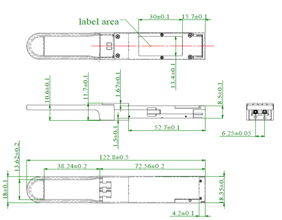
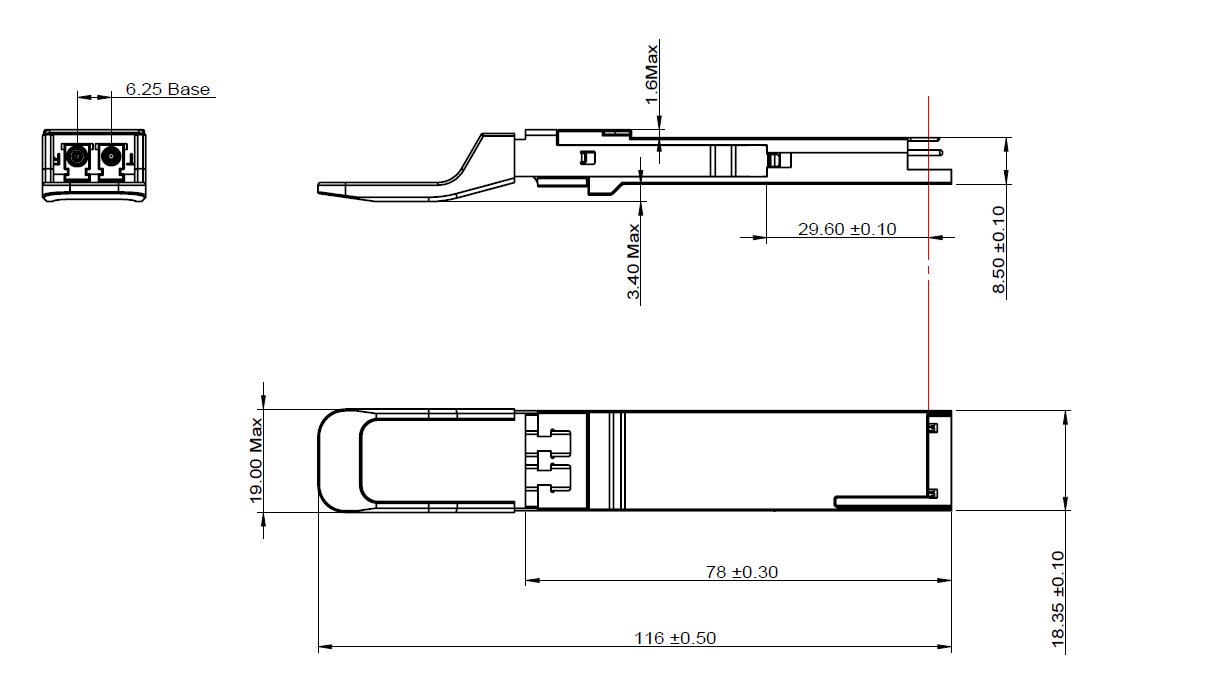
Mechanical Dimensions
Option 1:
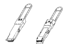
Option 2:
See LinkX® Memory Map Application Note (MLNX-15-5926).
An example of the label applied on the transceiver's back-shell is illustrated below.
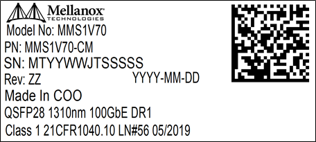
Images are for illustration purposes only. Product labels and colors may vary.
Transceiver Back-Shell Label Serial Number Legend
|
Symbol |
Meaning |
Notes |
|
MT |
Manufacturer name (Mellanox/NVIDIA) |
2 digits (alphanumeric) |
|
YY |
Year of manufacturing |
2 last digits of the year (numeric) |
|
WW |
Week of manufacturing |
2 digit (numeric) |
|
JT |
Manufacturer Site: JT (Taiwan) |
Two characters |
|
SSSSS |
Serial number |
5 digits (decimal numeric) for serial number, starting from 00001. |
|
MM |
Month |
2 digit (numeric) |
|
DD |
Day |
2 digit (numeric) |
|
ZZ |
Revision Number |
2 digits (alphanumeric) |