Pin Description
The device is OSFP MSA Specification for OSFP Octal Small Form Factor Pluggable Module Rev. 1.12 compliant, see www.osfpmsa.org.
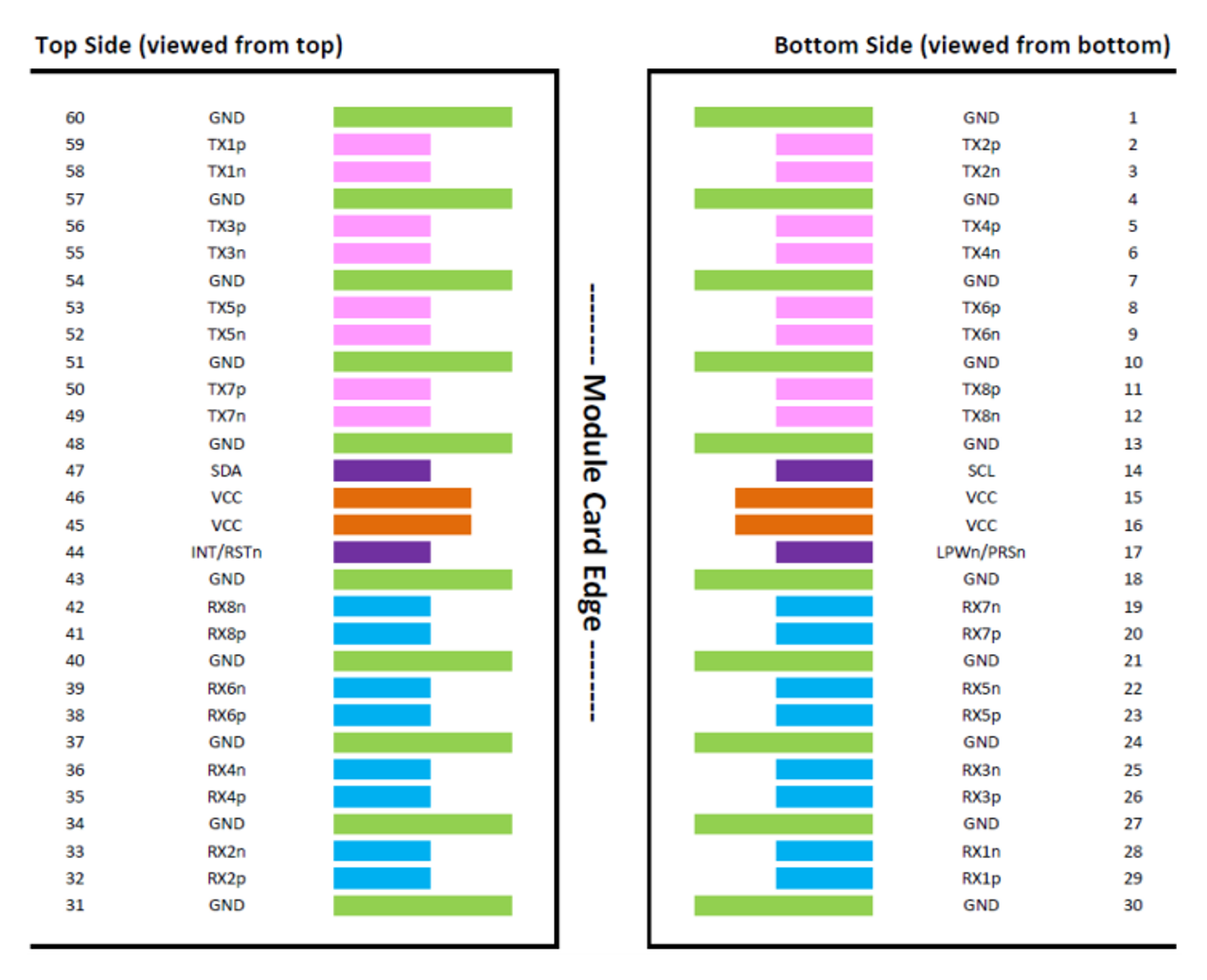
Pin | Symbol | Description | Pin | Symbol | Description |
1 | GND | Ground | 31 | GND | Ground |
2 | Tx2p | Transmitter Non-Inverted Data Input | 32 | Rx2p | Receiver Non-Inverted Data Output |
3 | Tx2n | Transmitter Inverted Data Input | 33 | Rx2n | Receiver Inverted Data Output |
4 | GND | Ground | 34 | GND | Grounds |
5 | Tx4p | Transmitter Non-Inverted Data Input | 35 | Rx4p | Receiver Non-Inverted Data Output |
6 | Tx4n | Transmitter Inverted Data Input | 36 | Rx4n | Receiver Inverted Data Output |
7 | GND | Ground | 37 | GND | Ground |
8 | Tx6p | Transmitter Non-Inverted Data Input | 38 | Rx6p | Receiver Non-Inverted Data Output |
9 | Tx6n | Transmitter Inverted Data Input | 39 | Rx6n | Receiver Inverted Data Output |
10 | GND | Ground | 40 | GND | Ground |
11 | Tx8p | Transmitter Non-Inverted Data input | 41 | Rx8p | Receiver Non-Inverted Data Output |
12 | Tx8n | Transmitter Inverted Data Input | 42 | Rx8n | Receiver Inverted Data Output |
13 | GND | Ground | 43 | GND | Ground |
14 | SCL | 2-wire serial interface clock | 44 | INT / RSTn | Module Interrupt / Module Reset |
15 | VCC | +3.3V Power | 45 | VCC | +3.3V Power |
16 | VCC | +3.3V Power | 46 | VCC | +3.3V Power |
17 | LPWn / PRSn | Low-Power Mode / Module Present | 47 | SDA | 2-wire Serial interface data |
18 | GND | Ground | 48 | GND | Ground |
19 | Rx7n | Receiver Inverted Data Output | 49 | Tx7n | Transmitter Inverted Data Input |
20 | Rx7p | Receiver Non-Inverted Data Output | 50 | Tx7p | Transmitter Non-Inverted Data Input |
21 | GND | Ground | 51 | GND | Ground |
22 | Rx5n | Receiver Inverted Data Output | 52 | Tx5n | Transmitter Inverted Data Input |
23 | Rx5p | Receiver Non-Inverted Data Output | 53 | Tx5p | Transmitter Non-Inverted Data Input |
24 | GND | Ground | 54 | GND | Ground |
25 | Rx3n | Receiver Inverted Data Output | 55 | Tx3n | Transmitter Inverted Data Input |
26 | Rx3p | Receiver Non-Inverted Data Output | 56 | Tx3p | Transmitter Non-Inverted Data Input |
27 | GND | Ground | 57 | GND | Ground |
28 | Rx1n | Receiver Inverted Data Output | 58 | Tx1n | Transmitter Inverted Data Input |
29 | Rx1p | Receiver Non-Inverted Data Output | 59 | Tx1p | Transmitter Non-Inverted Data Input |
30 | GND | Ground | 60 | GND | Ground |
OSFP Module Pad Layout
The Active Optical Cable (AOC) pin assignment is SFF-8679 compliant.
The transceivers are CMIS 4.0 compliant, management interface and OSFP 4.1 compliant form factor and interfaces. The control signals shown in the pad layout are implemented with the following functions:
Name | Function | Description |
LPWn/PRSn | Input/output | Multi-level signal for low power control from host to module and module presence indication from module to host. This signal requires the circuit as described in the OSFP Specification. |
INT/RSTn | Input,/output | Multi-level signal for interrupt request from module to host and reset control from host to module. This signal requires the circuit as described in the OSFP Specification. |
SCL | BiDir | 2-wire serial clock signal. Requires pull-up resistor to 3.3V on host. |
SDA | Bidir | 2-wire serial data signal. Requires pull-up resistor to 3.3V on host. |
The transceiver has a microcontroller with functions for monitoring supply voltage, temperature, laser bias current, optical transmit and receive levels with associated warning and alarm thresholds that can be read by the switch software and viewed remotely.
The transceiver supports the OSFP MSA specification and has the following key features:
Physical layer link optimization:
Adaptive Tx input equalization
Programmable Rx output amplitude
Programmable Rx output pre-cursor
Programmable Rx output post-cursor
Digital Diagnostic Monitoring (DDM):
Rx receive optical power monitor for each lane
Tx transmit optical power monitor for each lane
Tx bias current monitor for each lane
Supply voltage monitor
Transceiver case temperature monitor
Warning and Alarm thresholds for each DDM function (not user programmable)
Page 13h and 14h Module Diagnostics
Host side and line side loopback
PRBS generator and checker on host and line interfaces
Interrupt indications:
Tx & Rx LOS indication
Tx & Rx LOL indication
Tx fault indication
Other CMIS 4.0 functions
FW upgrade supported via CDB commands.