Specifications
Absolute maximum ratings are those beyond which the device may be damaged.
Parameter | Min | Max | Units |
Supply voltage | -0.3 | 3.6 | V |
Data input voltage | -0.3 | 3.6 | V |
Control input voltage | -0.3 | 3.6 | V |
This table shows the environmental specifications for the product.
Parameter | Min | Max | Units |
Storage temperature | -40 | 85 | °C |
This section shows the range of values for normal operation.
Parameter | Min | Typ | Max | Units |
Supply voltage (Vcc) | 3.135 | 3.3 | 3.465 | V |
Power consumption | --- | --- | 0.1 | W |
Operating case temperature | 0 | 70 | °C | |
Operating case temperature for MAM1Q00A-QSA_E | -10 | 85 | °C | |
Operating relative humidity | 5 | 85 | % |
Parameter | Min | Typ | Max | Units |
Characteristic Impedance | 90 | 100 | 110 | Ω |
This product is compatible with ESD levels in typical data center operating environments and certified in accordance with the standards listed in the Regulatory Compliance Section. The product is shipped with protective caps on all connectors to protect it during shipping. In normal handling and operation of high-speed cables and optical transceivers, ESD is of concern during insertion into the OSFP cage of the server/switch. Hence, standard ESD handling precautions must be observed. These include use of grounded wrist/shoe straps and ESD floor wherever a cable/transceiver is extracted/inserted. Electrostatic discharges to the exterior of the host equipment chassis after installation are subject to system level ESD requirements.
The figure below shows the dimensions of the QSA.
The SFP+/SFP mating paddle card dimension A10 (length of component/solder mask keep-out area, refer to SFF-8071) shall be >6.0mm instead of >5.5mm. The reason for this requirement is to prevent damaging the adapter when trying to insert an SFP upside down.
Mechanical Dimensions (Option 1)
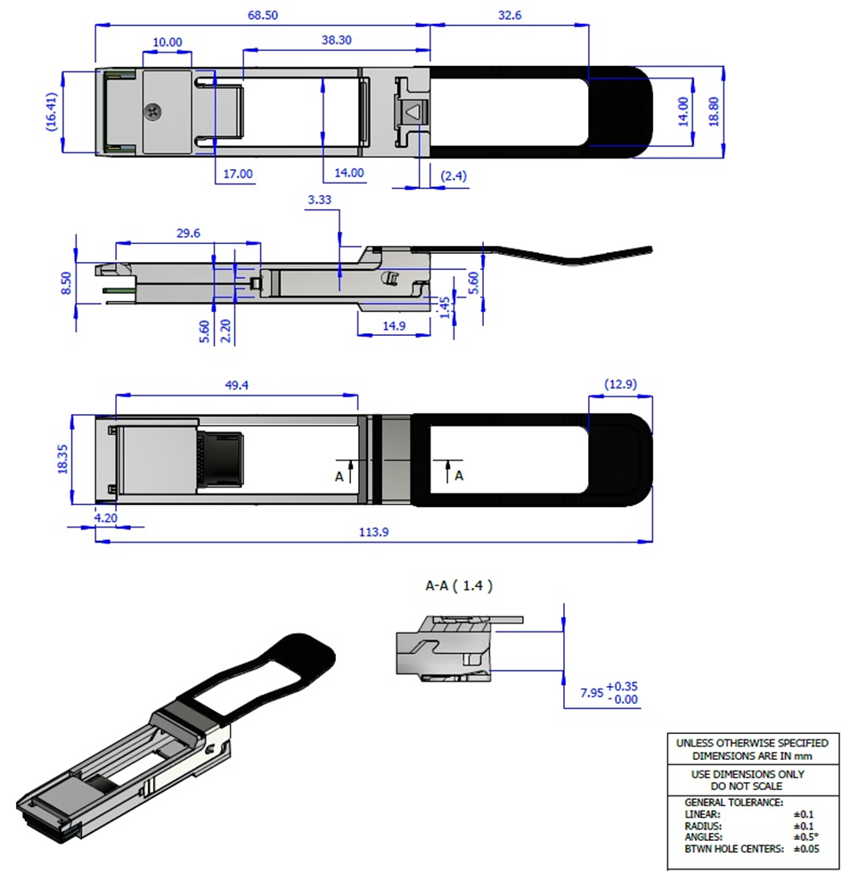
Dimensions provided in parenthesis are informative only and not a controlled dimension
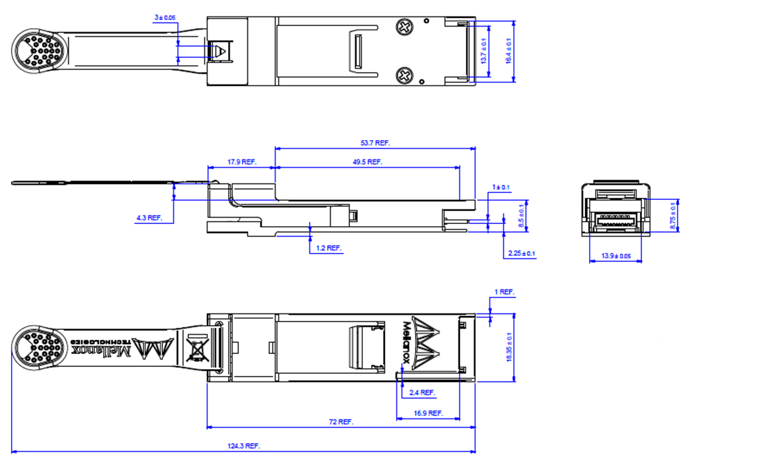
Mechanical Dimensions (Option 2)
RF Connectivity
QSFP+ Side | SFP/SFP+ Side |
TX1 | TX1 |
RX1 | RX1 |
TX2 | Terminated |
RX2 | Terminated |
TX3 | Terminated |
RX3 | Terminated |
TX4 | Terminated |
RX4 | Terminated |
The following label is applied on the cable’s backshell:
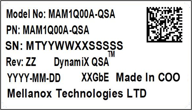
(sample illustration)
The following label is applied on the adapter’s pull-tab for option 2:
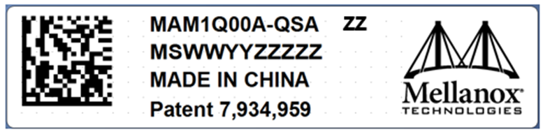
Legend: COO – Country of Origin
Backshell Label SN (Serial Number) Legend
Symbol | Meaning | Notes |
SN – Serial Number | ||
MT/MS | Manufacturer name | 2 characters, e.g. MT |
YY | Year of manufacturing | 2 digits |
WW | Week of manufacturing | 2 digits |
XX | Manufacturer site | 2 characters |
SSSSS | Serial number | 5 digits for serial number, starting from 00001. Reset at start of week to 00001. |
Miscellaneous | ||
ZZ | HW and SW revision | 2 alpha-numeric characters |
YYYY | Year of manufacturing | 4 digits |
MM | Month of manufacturing | 2 digits |
DD | Day of manufacturing | 2 digits |
COO | Country of origin | E.g. China or Malaysia |

| Quick response code | Serial number (MTYYWWXXSSSSS) |
Safety: CB, CE
EMC: CE, FCC, ICES, RCM
Ask your NVIDIA FAE for a zip file of the certifications for this product.
This equipment has been tested and found to comply with the limits for a Class A digital device, pursuant to part 15 of the FCC Rules. These limits are designed to provide reasonable protection against harmful interference when the equipment is operated in a commercial environment. This equipment generates, uses, and can radiate radio frequency energy and, if not installed and used in accordance with the instruction manual, may cause harmful interference to radio communications. Operation of this equipment in a residential area is likely to cause harmful interference in which case the user will be required to correct the interference at his own expense.