Open topic with navigation
Overview
Threads within a block can cooperate by sharing data through shared memory and by synchronizing their execution to coordinate memory accesses. Because it is on-chip, shared memory has much higher bandwidth and much lower latency than local or global memory. For that shared memory is equivalent to a user-managed cache: The application explicitly allocates and accesses it. A typical programming pattern is to stage data coming from device memory into shared memory, process the data in shared memory while sharing the shared view of the data across the threads of a block, and write the results back to device memory.
To achieve high bandwidth, shared memory is divided into equally-sized memory modules, called banks, which can be accessed simultaneously. Any memory read or write request made of n addresses that fall in n distinct memory banks can therefore be serviced simultaneously, yielding an overall bandwidth that is n times as high as the bandwidth of a single module. However, if two addresses of a memory request fall in the same memory bank, there is a bank conflict and the access has to be serialized. The hardware splits a memory request with bank conflicts into as many separate conflict-free requests as necessary, decreasing throughput by a factor equal to the number of separate memory requests. If the number of separate memory requests is n, the initial memory request is said to cause n-way bank conflicts. To get maximum performance, it is therefore important to understand how memory addresses map to memory banks in order to schedule the memory requests so as to minimize bank conflicts.
For devices of compute capability 2.x, shared memory has 32 banks that are organized such that successive 32bit words map to successive banks. Each bank has a bandwidth of 32 bits per two clock cycles. A shared memory request for a warp does not generate a bank conflict between two threads that access any address within the same 32bit word (even though the two addresses fall in the same bank). More details and examples of common access patterns are given in the Shared Memory section for compute capability 2.x in the CUDA C Programming Guide.
For devices of compute capability 3.x, shared memory has 32 banks with two addressing modes that can be configured using cudaDeviceSetSharedMemConfig(). Each bank has a bandwidth of 64 bits per clock cycle. In 64bit mode, successive 64bit words map to successive banks. A shared memory request for a warp does not generate a bank conflict between two threads that access any sub-word within the same 64bit word (even though the addresses of the two sub-words fall in the same bank). In 32bit mode (default), successive 32bit words map to successive banks. A shared memory request for a warp does not generate a bank conflict between two threads that access any sub-word within the same 32bit word or within two 32bit words whose indices i and j are in the same 64word aligned segment (i.e., a segment whose first index is a multiple of 64) and such that j=i+32 (even though the addresses of the two sub-words fall in the same bank). More details and examples of common access patterns are given in the Shared Memory section for compute capability 3.x in the CUDA C Programming Guide.
Chart
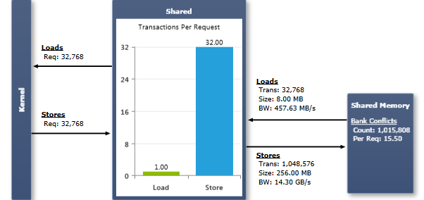
The number of Load/Store Requests equals the amount of shared memory instructions executed. When a warp executes an instruction that accesses shared memory, it resolves the bank conflicts as discussed previously. Each bank conflict forces a new memory transaction. The more transactions are necessary, the more unused words are transferred in addition to the words accessed by the threads, reducing the instruction throughput accordingly. Each memory transaction also requires the assembly instruction to be issued again; causing instruction replays if more than one transaction is required to fulfill the request of a warp. More details on instruction replays and their performance implications are described in the context of the Instruction Statistics experiment.
The Transactions Per Request chart shows the average number of shared memory transactions required per executed shared memory instruction, separately for load and store operations. Lower numbers are better; the target for a single shared memory operation on a full warp is 1 transaction for both, a 4byte access and an 8byte access, and 2 transactions for a 16byte access. Note that the ideal number of transactions for a given access pattern is dependent on the width of the access, the configured address mode (if available), and the target compute capability. Refer to the Ideal Shared Memory Transactions of the Memory Transactions experiment to tell the lowest number of transfers possible for a given instruction. The Transaction Size for shared memory traffic is 128 bytes for compute capability 2.x and 256 bytes for compute capability 3.x. For both devices classes the bandwidth is equal to one transaction per clock per SM.
|
Analysis
-
If the number of Transactions Per Request is high …
-
… run the Memory Transactions experiment to locate the source code lines that trigger shared memory operations. Check the used memory access patterns and try to optimize the data accesses with the goal of avoiding bank conflicts (see the Shared Memory sections of the CUDA C Programming Guide for more details).
-
… and the target device supports configuring the shared memory address mode, try switching the configuration and rerun the experiment. The CUDA Launches page reports the selected address mode configuration in the Shared Memory Configuration Executed column. In general the 64byte access mode is beneficial for all 8byte accesses. However certain access patterns optimized for the 32byte mode incur additional bank conflicts in the 64byte mode; hence choosing the best address mode requires understanding the count, width, and access pattern for all executed shared memory instructions.
-
If the number of Load/Store Requests is high …
-
… and the target device is of compute capability 3.x, investigate if shared memory accesses can be replaced with shuffle operations. This new warp-level intrinsic allows the threads of a warp to exchange data with each other directly without going through shared (or global) memory. The shuffle instruction also has lower latency than shared memory access and does not consume shared memory space for data exchange, so this can present an attractive way for applications to rapidly interchange data among threads.
NVIDIA GameWorks Documentation Rev. 1.0.150630 ©2015. NVIDIA Corporation. All Rights Reserved.