Interfaces
Each Mellanox Innova-2 Flex Open adapter card may include some or all of the interfaces described in this chapter, as well as special circuits to protect from ESD shocks to the card/server when plugging copper cables.
The network ports of the adapter cards are compliant with the InfiniBand Architecture Specification, Release 1.3. InfiniBand traffic is transmitted through the SFP28 connectors on MNV303212A-ADLT, or QSFP28 connectors on MNV303611A-EDLT.
The network ports of the adapter cards are compliant with the IEEE 802.3 Ethernet standards listed in the Features table. The MNV303212A-ADLT interface provides two SFP28 ports of 10/25Gb/s, and the MNV303611A-EDLT provides two QSFP28 ports of 40/100Gb/s through the ConnectX-5 adapter. The FPGA does not have direct access to this interface.
The adapter cards support PCI Express Gen 3.0/4.0 through an x8 edge connector. The device can be either a master initiating the PCI Express bus operations or a slave responding to PCI bus operations. For pinout of the PCIe interface, please refer to the attached Mellanox Innova-2 Flex Open Interface Pinouts or to the attached Verilog and XDC files.
Network LEDs Operation
LEDs D1 and D2 provide information on ConnectX-5 Port 1 and Port 2, respectively. The following table defines the LED behavior.
LED | Function |
Off | A link has not been established |
Blinking Ambera | 6 Hz blinking Amber indicates a problem with the link |
Solid Green | Indicates a valid link with no active traffic |
Blinking Green | Indicates a valid logical link with active traffic |
a. 1 Hz Blinking Amber occurs due to running a beacon command for locating the adapter card.
FPGA LEDs Indications
LED Name | FPGA Pinout | Function |
D18 | A6 | For User Image: Programmable For Mellanox Innova-2 Flex Open Image: DDR clock blink |
D19 | B6 | For User Image: Programmable For Mellanox Innova-2 Flex Open Image: DDR HW BIST status (on - success, off - failure/in progress) |
General LEDs Indications
LED Name | Function |
D10 | On when ConnectX power is stable |
D15 | Red when PROG_B or DONE are low. Green when Done is high |
JTAG interface is used for direct connection to Xilinx development tools through a JTAG cable, for FPGA configuration. This interface is only intended as a hardware backup when there is no other way to configure the FPGA. See Xilinx Programming Cable.
This section applies to MNV303212A-ADLT only.
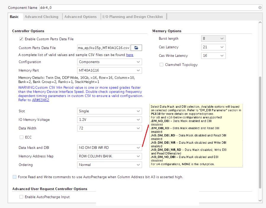
The Mellanox Innova-2 Flex Open adapter supports up to 8GB DDR4 FPGA dedicated memory with a single channel 64b + 8b ECC interface. The memory is ECC protected. When working with Xilinx DDR4 controller, it is recommended to enable the DBI option by default by selecting “NO DM DBI WR RD” as shown in the following figure.
For further details, please refer to DDR4 controller documentation listed in Recommended Documents and Tools.
For pinout of the DDR4 interface, please refer to the attached Mellanox Innova-2 Flex Open Interface Pinouts or to the attached Verilog and XDC files.
Importing CSV Inputs from Vivado
To import CSV inputs from Vivado when generating the DDR4 IP Core, please perform the following steps:
In the Project Manager navigation panel, click on IP Catalog.

Under Vivado Repository, click on Memories & Storage Elements → External Memory Interface, and select DDR4 SDRAM (MIG).

Choose a name for your IP (ddr4), and type it in the Component Name field.


In the Basic tab under Mode and Interface, select Controller and physical layer. The AXI4 Interface can be added by checking the adjacent checkbox.

Under Clocking:
In the Memory Device Interface Speed (ps) field, select 833 (1200MHz, to run the DDR at 2400MHz).
In the Reference Input Clock Speed (ps) field, select 9996 (100.04MHz), which is the DDR clock on the board.

Under Controller Options, check the Enable Custom Parts Data File checkbox, and upload the CSV file that is attached to this document. In the Memory Part drop-down menu, select MT40A1G16, and in Data Mask and DBI, it is recommended to select "NO DM DBI WR RD" = Data Mask disabled, Write and Read DBI enabled. The other parameters are set by the CSV file.
Note that the ECC checkbox is checked following the AXI4 I/F selection (the data should include the ECC).
Additional Recommendations
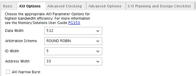
In the AXI Options tab, customize the fields as follows:
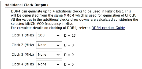
Under Additional Clock Outputs, customize the fields as follows:
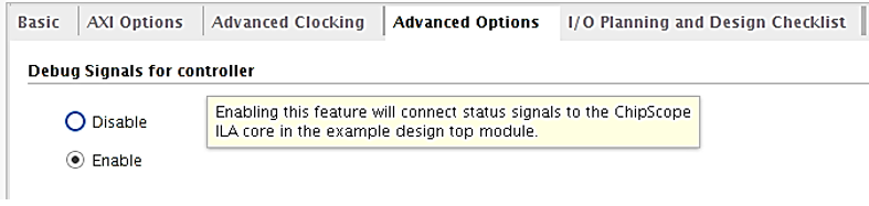
In the Advanced Options tab, under Debug Signals for Controller select Enable.
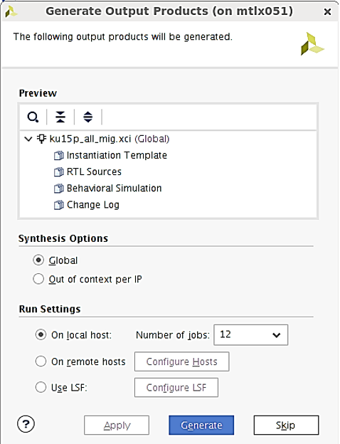
Click OK and select
Global for Synthesis Options:
The FPGA is connected to the ConnectX-5 embedded PCIe Gen3 x8 switch and is accessible both from the ConnectX-5 and the host over the PCIe interface. PCI reset to the FPGA is driven by the ConnectX-5 adapter.
The FPGA is connected to two x4 on-board MICRON TECHNOLOGY (MT25QU512ABB8E12-0SIT) QSPI flashes.
Signal | Total Delay |
D0 | 0.35135232 |
D1 | 0.355097342 |
D2 | 0.35009532 |
D3 | 0.353372756 |
CS0# | 0.350112638 |
CCLK | 0.355390305 |
D4 | 0.268570741 |
D5 | 0.263691389 |
D6 | 0.266098594 |
D7 | 0.265581939 |
CS1# | 0.266061071 |
CCLK | 0.268427867 |
Clock | Pin Number |
DDR CLK 100.04MHz LVDS (in MNV303212A-ADLT only) | AP24 (P), AP25 (N) |
EMCCLK 150MHz LVCMOS | AM14 |
SYSCLK 100MHz LVDS | AR14 (P), AT14 (N) |
PCIe internal link 100MHz LVDS | AB27 (P), AB28 (N) [GTY128 CLK0] |
For further details, please refer to DDR4 controller documentation listed in Recommended Documents and Tools.
For pinout of the DDR4 interface, please refer to the attached Mellanox Innova-2 Flex Open Interface Pinouts or to the attached Verilog and XDC files.