Specifications
Absolute maximum ratings are those beyond which damage to the device may occur.
Prolonged operation between the operational specifications and absolute maximum ratings is not intended and may cause permanent device degradation.
Parameter | Min | Max | Units |
Supply voltage | -0.3 | 3.6 | V |
Data input voltage | -0.3 | 3.6 | V |
Control input voltage | -0.3 | 3.6 | V |
This table shows the environmental specifications for the product.
Parameter | Min | Max | Units |
Storage temperature | -40 | 85 | °C |
This section shows the range of values for normal operation.
Parameter | Min | Typ | Max | Units |
Supply voltage (Vcc) | 3.135 | 3.3 | 3.465 | V |
Power consumption | --- | --- | 0.1 | W |
Operating case temperature | 0 | 70 | °C | |
Operating relative humidity | 5 | 85 | % |
Parameter | Min | Typical | Max | Units |
Characteristic impedance | 90 | 100 | 110 | Ω |
Time propagation delay | --- | --- | 4.5 | ns/m |
Optical Module Specifications
Page 00h/ | Register Name | Description |
0-1 | Identifier | 03: SFP/SFP+/SFP28 |
1 | Extended Identifier | 04h: 2-wire interface |
2 | Connector | 23h: Direct attach assemblies with no separable interfaces |
8 | Cable Technology | 04h: Passive cable |
18 | Length | Length in units of 1 m of direct attach copper cable. |
20-35 | Vendor name | NVIDIA: ASCII |
36 | Link codes | 0Bh: CA-L (Cable Assembly FEC) |
37-39 | QSFP vendor IEEE number | 00-02-C9: Mellanox OUI. |
40-55 | Part number | MCP7F00-A0xxEyyz: Part number per backshell label (ASCII) |
57-59 | Product revision | ZZ: Revision per backshell label (ASCII) |
68-83 | Serial number | MTYYWWXXSSSSS: Serial number per backshell label. |
84-89 | Date code | YYMMDD: Year YY, month MM, day DD. |
94 | Compliance | 08h: SFF-8472 Compliance |
108 | Length 0.1m | Total cable length is the sum of byte 18 for number of meters and byte 108 for 0.1m. Values: Examples: |
109 | AWG | DAC cable AWG information. |
Please note that the MCP2M00 is a passive cable, and therefore has no Digital Diagnostic Monitoring (DDM) functions implemented. However, it is considered compliant with SFF-8472 to enable the host system to read device declarations including interconnect type, link code, and cable length. The compliance and DDM declarations are interpreted as follows:
Read address 94 = 08h. This declares SFF-8472 rev. 12.3 compliance.
Read address 92 bit 6 = 0. This declares that DDM is NOT implemented. This declaration contradicts the wording of SFF-8472 rev. 12.3, but it prevents the host system from hanging if attempting to access the unimplemented upper page A2h.
Cable Length (m) | AWG | Single Cable Diameter (mm) | Minimum Bend Radius | Color | |
MCP2M00-A02AE30L | 2.5 | 30 | 4.5 ±0.2 | Single bend: 21mm Assembly/Repeated bend: 45mm | Black |
MCP2M00-A003E30L | 3 | ||||
MCP2M00-A00AE30N | 0.5 | ||||
MCP2M00-A001E30N | 1 | ||||
MCP2M00-A01AE30N | 1.5 | ||||
MCP2M00-A002E30N | 2 | ||||
MCP2M00-A004E26L | 4 | 26 | 5.8 +0.3/ | Single bend: 29mm Repeated bend: 58mm | |
MCP2M00-A005E26L | 5 | ||||
MCP2M00-A02AE26N | 2.5 | ||||
MCP2M00-A003E26N | 3 |
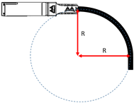
The minimum assembly bending radius (close to the connector) is 10x the cable’s outer diameter. The repeated bend (far from the connector) is also 10x the cable’s outer diameter. The single bend (far from the connector) is 5x the cable’s outer diameter.
Mechanical Dimensions
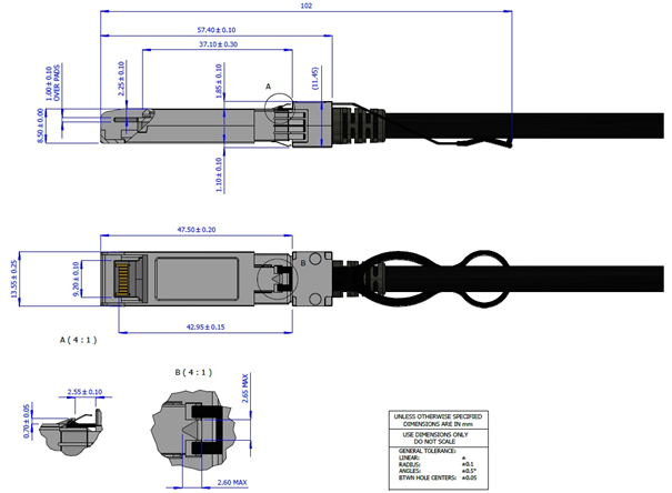
Assembly Bending Radius
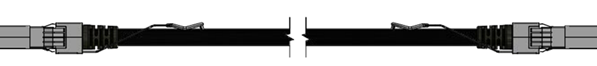
Cable Length Definition

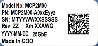
The following label is applied on the cable’s backshell:
Backshell Label (Example)
(sample illustration)
Backshell Label Legend
Symbol | Meaning | Notes |
SN – Serial Number | ||
MT | Manufacturer name | 2 characters, e.g. MT |
YY | Year of manufacturing | 2 digits |
WW | Week of manufacturing | 2 digits |
XX | Manufacturer site | 2 characters |
SSSSS | Serial number | 5 digits for serial number, starting from 00001. Reset at start of week to 00001. |
Miscellaneous | ||
ZZ | HW and SW revision | 2 alpha-numeric characters |
YYYY | Year of manufacturing | 4 digits |
MM | Month of manufacturing | 2 digits |
DD | Day of manufacturing | 2 digits |
COO | Country of origin | E.g. China or Malaysia |

| Quick response code | Serial number (MTYYWWXXSSSSS) |
Copper Cable Jacket Label Example

(sample illustration)
Notes: Serial number and barcode are for NVIDIA internal use only.
Images are for illustration purposes only. Product labels, colors, and lengths may vary.
Safety: CB, UL, CE
EMC: CE, FCC, ICES, RCM, VCCI
Ask your NVIDIA FAE for a zip file of the certifications for this product.
Each of the devices complies with CFR47 FCC Class A Part 15 of the FCC Rules. Operation is subject to the following two conditions:
This device may not cause harmful interference.
This device must accept any interference received, including interference that may cause undesired
Note: This equipment has been tested and found to comply with the limits for a Class A digital device, pursuant to Part 15 of the FCC Rules. These limits are designed to provide reasonable protection against harmful interference in a residential installation. This equipment generates, uses and can radiate radio frequency energy and, if not installed and used in accordance with the instructions, may cause harmful interference to radio communications. However, there is no guarantee that interference will not occur during installation. If this equipment does cause harmful interference to radio or television reception, which can be determined by turning the equipment off and on, the user is encouraged to try to correct the interference by one or more of the following measures:
Reorient or relocate the receiving antenna.
Increase the separation between the equipment and receiver.
Connect the equipment into an outlet on a circuit different from that to which the receiver is connected.
Consult the dealer or an experienced radio/television technician for help.
Modifications: Any modifications made to this device that are not approved by NVIDIA may void the authority granted to the user by the FCC to operate this equipment.