Specifications
Absolute maximum ratings are those beyond which damage to the device may occur.
Prolonged operation between the operational specifications and absolute maximum ratings is not intended and may cause permanent device degradation.
|
Parameter |
Min |
Max |
Units |
|
Supply voltage |
-0.3 |
3.6 |
V |
|
Data input voltage |
-0.3 |
3.6 |
V |
|
Control input voltage |
-0.3 |
3.6 |
V |
This table shows the environmental specifications for the product.
|
Parameter |
Min |
Max |
Units |
|
Storage temperature |
-40 |
85 |
°C |
This section shows the range of values for normal operation.
|
Parameter |
Min |
Typ |
Max |
Units |
|
Supply voltage (Vcc) |
3.135 |
3.3 |
3.465 |
V |
|
Power consumption |
--- |
--- |
0.1 |
W |
|
Operating case temperature |
0 |
70 |
°C |
|
|
Operating relative humidity |
5 |
85 |
% |
|
Parameter (per lane) |
Min |
Typ |
Max |
Units |
Notes |
|
Characteristic Impedance |
90 |
100 |
110 |
Ω |
--- |
|
Time propagation delay |
--- |
--- |
4.5 |
ns/m |
Informative |
Note: Minimum insertion loss for up to 1m cable length is 6dB @ 12.89GHz.
This product is compatible with ESD levels in typical data center operating environments and certified in accordance with the standards listed in the Regulatory Compliance Section. The product is shipped with protective caps on all connectors to protect it during shipping. In normal handling and operation of high-speed cables and optical transceivers, ESD is of concern during insertion into the QSFP cage of the server/switch. Hence, standard ESD handling precautions must be observed. These include use of grounded wrist/shoe straps and ESD floor wherever a cable/transceiver is extracted/inserted. Electrostatic discharges to the exterior of the host equipment chassis after installation are subject to system level ESD requirements.
The head-end of the MCP7H50 cable is QSFP-DD. Hence the memory map of its EEPROM is formatted in compliance with CMIS 4.0. The key parameters are listed below. The EEPROMs of the QSFP ‘tails’ are SFF-8636 compliant. The memory map of the QSFPs is found in the QSFP56 Memory Map – SFF-8636 compliant - I2C Address A0h table .
QSFP56 Memory Map – SFF-8636 compliant - I2C Address A0h
|
Page 00h/ Dec. Byte Address |
Register Name |
Description |
|
0 |
Identifier |
11h: QSFP28 or later |
|
1 |
Status |
08h: Support for SFF-8636 Rev. 2.8 and 2.9 |
|
113 |
Far/near end implementation |
50h: 4x side 1Ch: 2x side |
|
128 |
Identifier |
11h: QSFP28 or later |
|
130 |
Connector |
23h: Direct attach assemblies with no separable interfaces |
|
139 |
Code for Serial Encoding Algorithm |
08h: PAM4 |
|
146 |
Length |
Length in units of 1 m of direct attach copper cable (integer part – see byte Address 236) |
|
147 |
Device technology |
A0h: Un-equalized copper cable (passive) |
|
148-163 |
Vendor name |
NVIDIA: ASCII |
|
164 |
Extended Module Codes Values |
3Fh: InfiniBand HDR |
|
165-167 |
QSFP vendor IEEE number |
00-02-C9: NVIDIA OUI. |
|
168-183 |
Part number |
MCP7H50-H0xxRyy: Part number per backshell label (ASCII) |
|
184-185 |
Product revision |
ZZ: Revision per backshell label (ASCII) |
|
186 |
Attenuation 2.5 GHz |
Typical attenuation measured during production test, in 1dB. [dB] |
|
187 |
Attenuation 5 GHz |
|
|
188 |
Attenuation 7 GHz |
|
|
189 |
Attenuation 12.9 GHz |
|
|
190 |
Max case temperature |
46h: Support for 70ºC |
|
192 |
Link codes |
40h: 50GBASE-CR, 100GBASE-CR2, or 200GBASE-CR4 |
|
196-211 |
Serial number |
MTYYWWXXSSSSS: Serial number per backshell label (ASCII). |
|
212-217 |
Date code |
YYMMDD: Year YY, month MM, day DD. |
|
222 |
Extended signaling rate |
6Ah: Nominal signaling rate per channel, units of 250 MBd. |
|
236 |
Length 0.1m |
Total cable length is the sum of byte 146 for number of meters and byte 236 for 0.1m. Values: 00h: 0m … 09h: 0.9m Examples: 2.5m: Byte 146 = 02h, Byte 236 = 05h 2.25m: Byte 146 = 02h, Byte 236 = 03h |
|
237 |
AWG |
DAC cable AWG information. 18h: AWG=24 19h: AWG=25 1Ah: AWG=26 1Ch: AWG=28 1Eh: AWG=30 20h: AWG=32 |
|
AWG |
Single Cable Diameter |
Minimum Bend Radius |
Length Tolerance |
Cable Color |
|
|
MCP7H50-H001R30 |
30 |
5.2 +/-0.35mm |
Single bend: 28mm Repeated bend: 56mm |
+/-25mm |
Black |
|
MCP7H50-H01AR30 |
|||||
|
MCP7H50-V002R26 |
26 |
6.8 +/- 0.3mm |
Single bend: 34mm Repeated bend: 74mm |
+/-50mm |
* Assembly space calculation is based on repeated bend radius.
Pull-tab Colors
|
Single 200Gb/s QSFP56 Side |
|
|
Black |
|
|
Dual 100Gb/s QSFP56 Side |
|
|
Port 1: Green |
Port 2: Blue |
|
Promo Green |
Nice Blue |
|
Hex = #6faa55 |
Hex = #3b5998 |
|
RGB = 111, 170, 85 |
RGB = 59, 89, 152 |
|
CMYK = 52, 0, 86, 0 |
CMYK = 86, 64, 10, 0 |
|
Pantone = 368 Coated / 368 Uncoated |
Pantone = 660 Coated / 661 Uncoated |
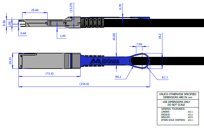
Mechanical Dimensions
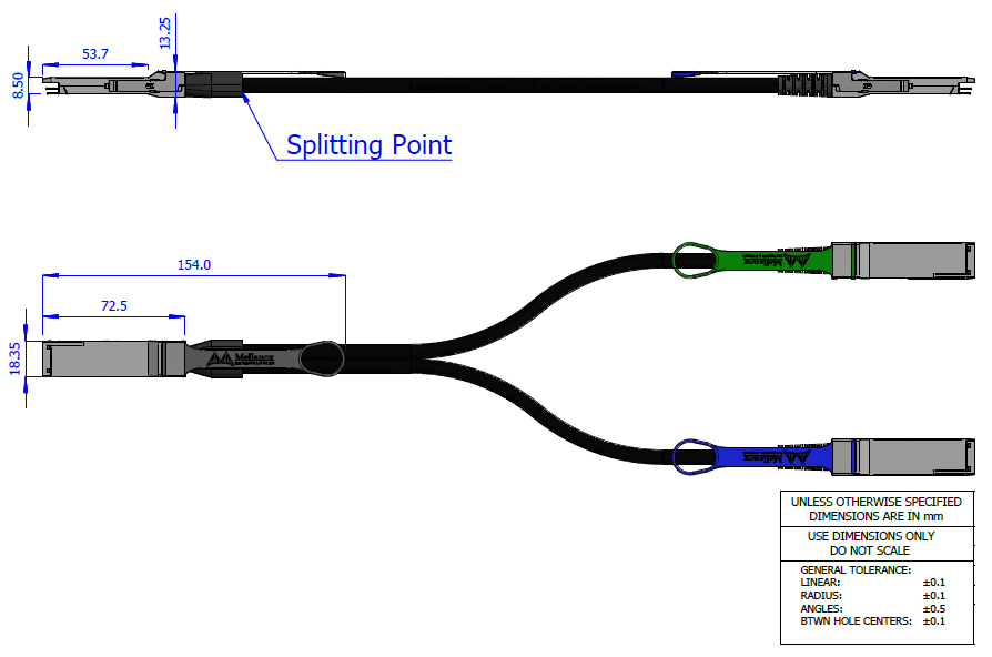
Mechanical Dimensions QSFP56
*Ordered OPN length.
Connectivity Schematic
|
200Gb/s QSFP56 Side |
100Gb/s 2xQSFP56 Side |
|
Port 1 Green |
|
|
TX1 |
RX1 |
|
RX1 |
TX1 |
|
TX2 |
RX2 |
|
RX2 |
TX2 |
|
Port 2 Blue |
|
|
TX3 |
RX1 |
|
RX3 |
TX1 |
|
TX4 |
RX2 |
|
RX4 |
TX2 |
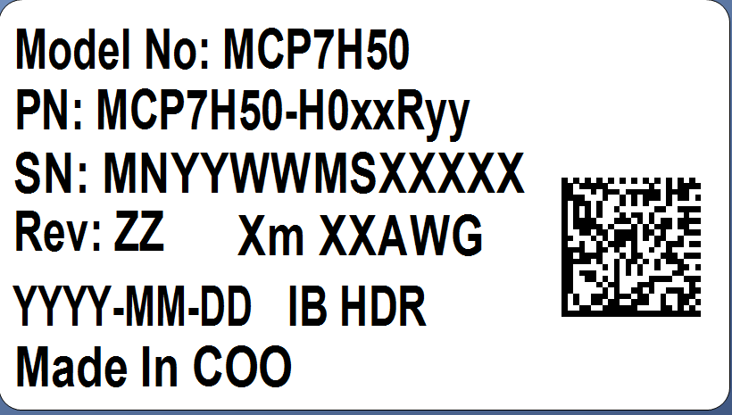
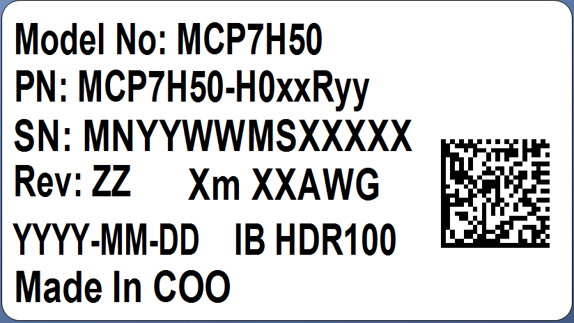
The following label is applied on the cable’s backshell:
Backshell Label 200Gb/s QSFP56
(sample illustration)
Backshell Label 100Gb/s QSFP56
(sample illustration)
Legend: COO – Country of Origin
The following label is applied on the cable’s jacket:
Copper Cable Jacket Label
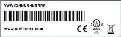
(sample illustration)
The following labels are applied on the cable’s jacket at the tail:
Splitter Copper Cable Labels Identifying the Tails
(sample illustration)
Splitter Copper Cable Label Defining the Data Rate of Each Tail

Backshell Label Legend
|
Symbol |
Meaning |
Notes |
|
SN – Serial Number |
||
|
MT |
Manufacturer name |
2 characters, e.g. MT |
|
YY |
Year of manufacturing |
2 digits |
|
WW |
Week of manufacturing |
2 digits |
|
XX |
Manufacturer site |
2 characters |
|
SSSSS |
Serial number |
5 digits for serial number, starting from 00001. Reset at start of week to 00001. |
|
Miscellaneous |
||
|
ZZ |
HW and SW revision |
2 alpha-numeric characters |
|
YYYY |
Year of manufacturing |
4 digits |
|
MM |
Month of manufacturing |
2 digits |
|
DD |
Day of manufacturing |
2 digits |
|
COO |
Country of origin |
E.g. China or Malaysia |

|
Quick response code |
Serial number (MTYYWWXXSSSSS) |
The MCP7H50 is qualified in accordance with the following standards:
Safety: CB, UL, CE
EMC: CE, FCC, ICES, RCM,VCCI
Ask your NVIDIA field engineer or the support team for a zip file of the certifications for this product.
Each of the devices complies with CFR47 FCC Class A Part 15 of the FCC Rules. Operation is subject to the following two conditions:
This device may not cause harmful interference.
This device must accept any interference received, including interference that may cause undesired
Note: This equipment has been tested and found to comply with the limits for a Class A digital device, pursuant to Part 15 of the FCC Rules. These limits are designed to provide reasonable protection against harmful interference in a residential installation. This equipment generates, uses and can radiate radio frequency energy and, if not installed and used in accordance with the instructions, may cause harmful interference to radio communications. However, there is no guarantee that interference will not occur during installation. If this equipment does cause harmful interference to radio or television reception, which can be determined by turning the equipment off and on, the user is encouraged to try to correct the interference by one or more of the following measures:
Reorient or relocate the receiving antenna.
Increase the separation between the equipment and receiver.
Connect the equipment into an outlet on a circuit different from that to which the receiver is connected.
Consult the dealer or an experienced radio/television technician for help.
Modifications: Any modifications made to this device that are not approved by NVIDIA may void the authority granted to the user by the FCC to operate this equipment.