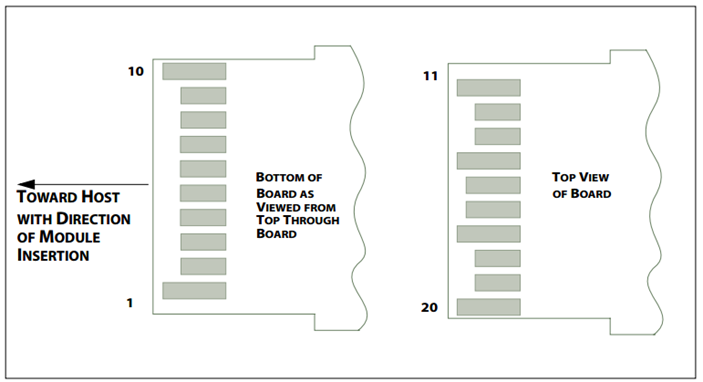
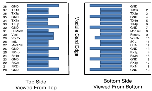
Pin Descriptions
The pin assignment is SFF-8679 compliant.
Pin | Symbol | Description | Pin | Symbol | Description |
1 | GND | Ground | 20 | GND | Ground |
2 | Tx2n | Transmitter Inverted Data Input | 21 | Rx2n | Receiver Inverted Data Output |
3 | Tx2p | Transmitter Non-Inverted Data Input | 22 | Rx2p | Receiver Non-Inverted Data Output |
4 | GND | Ground | 23 | GND | Grounds |
5 | Tx4n | Transmitter Inverted Data Input | 24 | Rx4n | Receiver Inverted Data Output |
6 | Tx4p | Transmitter Non-Inverted Data Input | 25 | Rx4p | Receiver Non-Inverted Data Output |
7 | GND | Ground | 26 | GND | Ground |
8 | ModSelL | Module Select | 27 | ModPrsL | Module Present |
9 | ResetL | Module Reset | 28 | IntL | Interrupt |
10 | Vcc Rx | +3.3V Power Supply Receiver | 29 | Vcc Tx | +3.3V Power Supply Transmitter |
11 | SCL | 2-wire Serial Interface Clock | 30 | Vcc1 | +3.3V Power Supply |
12 | SDA | 2-wire Serial Interface Data | 31 | LPMode | Low Power Mode |
13 | GND | GND | 32 | GND | Ground |
14 | Rx3p | Receiver Non-Inverted Data Output | 33 | Tx3p | Transmitter Non-Inverted Data Input |
15 | Rx3n | Receiver Inverted Data Output | 34 | Tx3n | Transmitter Inverted Data Input |
16 | GND | Ground | 35 | GND | Ground |
17 | Rx1p | Receiver Non-Inverted Data Output | 36 | Tx1p | Transmitter Non-Inverted Data Input |
18 | Rx1n | Receiver Inverted Data Output | 37 | Tx1n | Transmitter Inverted Data Input |
19 | GND | Ground | 38 | GND | Ground |
QSFP56 Module Pad Layout
Pin | Symbol | Description |
1 | VeeT | Module Transmitter Ground |
2 | Tx_Fault | Module Transmitter Fault. Connected to GND. |
3 | Tx_Disable | Not used. Connected to 3.3V |
4 | SDA | 2-wire Serial Interface Data Line |
5 | SCL | 2-wire Serial Interface Clock |
6 | Mod_ABS | Module Absent. Grounded within the module |
7 | RS0 | Rate Select 0, optionally controls SFP+ module receiver. Pulled down to GND. Not used. |
8 | Rx_LOS | Not used. Connected to GND. |
9 | RS1 | Rate Select 1, optionally controls SFP+ module transmitter. Not used. |
10 | VeeR | Module Receiver Ground |
11 | VeeR | Module Receiver Ground |
12 | RD- | Receiver Inverted Data Output |
13 | RD+ | Receiver Non-Inverted Data Output |
14 | VeeR | Module Receiver Ground |
15 | VccR | Module Receiver Power Supply |
16 | VccT | Module Transmitter Power Supply. Connected to 3.3V. |
17 | VeeT | Module Transmitter Ground |
18 | TD+ | Transmitter Non-Inverted Data Input. AC coupled |
19 | TD- | Transmitter Inverted Data Input. AC coupled |
20 | VeeT | Module Transmitter Ground |
SFP56 Module Pad Layout