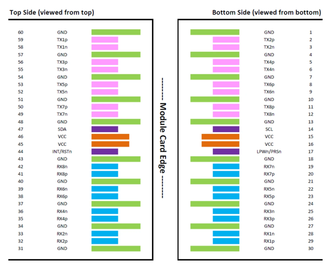
Pin Descriptions
The device is OSFP based (Octal Small Form Factor Pluggable, www.osfpmsa.org).
The pin assignment for the interface is shown below.
|
Pin |
Symbol |
Description |
Pin |
Symbol |
Description |
|
1 |
GND |
Ground |
31 |
GND |
Ground |
|
2 |
Tx2p |
Transmitter Non-Inverted Data Input |
32 |
Rx2p |
Receiver Non-Inverted Data Output |
|
3 |
Tx2n |
Transmitter Inverted Data Input |
33 |
Rx2n |
Receiver Inverted Data Output |
|
4 |
GND |
Ground |
34 |
GND |
Grounds |
|
5 |
Tx4p |
Transmitter Non-Inverted Data Input |
35 |
Rx4p |
Receiver Non-Inverted Data Output |
|
6 |
Tx4n |
Transmitter Inverted Data Input |
36 |
Rx4n |
Receiver Inverted Data Output |
|
7 |
GND |
Ground |
37 |
GND |
Ground |
|
8 |
Tx6p |
Transmitter Non-Inverted Data Input |
38 |
Rx6p |
Receiver Non-Inverted Data Output |
|
9 |
Tx6n |
Transmitter Inverted Data Input |
39 |
Rx6n |
Receiver Inverted Data Output |
|
10 |
GND |
Ground |
40 |
GND |
Ground |
|
11 |
Tx8p |
Transmitter Non-Inverted Data Input |
41 |
Rx8p |
Receiver Non-Inverted Data Output |
|
12 |
Tx8n |
Transmitter Inverted Data Input |
42 |
Rx8n |
Receiver Inverted Data Output |
|
13 |
GND |
Ground |
43 |
GND |
Ground |
|
14 |
SCL |
2-wire serial interface clock |
44 |
INT / RSTn |
Module Interrupt / Module Reset |
|
15 |
VCC |
+3.3V Power |
45 |
VCC |
+3.3V Power |
|
16 |
VCC |
+3.3V Power |
46 |
VCC |
+3.3V Power |
|
17 |
LPWn / PRSn |
Low-Power Mode / Module Present |
47 |
SDA |
2-wire Serial interface data |
|
18 |
GND |
Ground |
48 |
GND |
Ground |
|
19 |
Rx7n |
Receiver Inverted Data Output |
49 |
Tx7n |
Transmitter Inverted Data Input |
|
20 |
Rx7p |
Receiver Non-Inverted Data Output |
50 |
Tx7p |
Transmitter Non-Inverted Data Input |
|
21 |
GND |
Ground |
51 |
GND |
Ground |
|
22 |
Rx5n |
Receiver Inverted Data Output |
52 |
Tx5n |
Transmitter Inverted Data Input |
|
23 |
Rx5p |
Receiver Non-Inverted Data Output |
53 |
Tx5p |
Transmitter Non-Inverted Data Input |
|
24 |
GND |
Ground |
54 |
GND |
Ground |
|
25 |
Rx3n |
Receiver Inverted Data Output |
55 |
Tx3n |
Transmitter Inverted Data Input |
|
26 |
Rx3p |
Receiver Non-Inverted Data Output |
56 |
Tx3p |
Transmitter Non-Inverted Data Input |
|
27 |
GND |
Ground |
57 |
GND |
Ground |
|
28 |
Rx1n |
Receiver Inverted Data Output |
58 |
Tx1n |
Transmitter Inverted Data Input |
|
29 |
Rx1p |
Receiver Non-Inverted Data Output |
59 |
Tx1p |
Transmitter Non-Inverted Data Input |
|
30 |
GND |
Ground |
60 |
GND |
Ground |
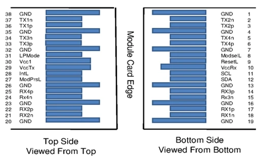
OSFP Module Pad Layout
|
Pin |
Symbol |
Description |
Pin |
Symbol |
Description |
|
1 |
Ground |
Ground |
20 |
Ground |
Ground |
|
2 |
Tx2n |
Connected to Port 1 lane Rx2 Inverted Data |
21 |
Rx2n |
Connected to Port 1 lane Tx2 Inverted Data |
|
3 |
Tx2p |
Connected to Port 1 lane Rx2 Non-Inverted Data |
22 |
Rx2p |
Connected to Port 1 lane Tx2 Non-Inverted Data |
|
4 |
Ground |
Ground |
23 |
Ground |
Grounds |
|
5 |
Tx4n |
Connected to Port 2 lane Rx2 Non-Inverted Data |
24 |
Rx4n |
Connected to Port 2 lane Tx2 Inverted Data |
|
6 |
Tx4p |
Connected to Port 2 lane Rx2 Inverted Data |
25 |
Rx4p |
Connected to Port 2 lane Tx2 Non-Inverted Data |
|
7 |
Ground |
Ground |
26 |
Ground |
Ground |
|
8 |
Mod-SelL |
Cable Select |
27 |
ModPrsL |
Cable Present |
|
9 |
ResetL |
Cable Reset |
28 |
IntL |
Interrupt |
|
10 |
Vcc Rx |
+3.3V Power supply receiver |
29 |
Vcc Tx |
+3.3V Power supply transmitter |
|
11 |
SCL |
2-wire serial interface clock |
30 |
Vcc1 |
+3.3V Power Supply |
|
12 |
SDA |
2-wire serial interface data |
31 |
LPMode |
Low Power Mode |
|
13 |
Ground |
Ground |
32 |
Ground |
Ground |
|
14 |
Rx3p |
Connected to Port 2 lane Tx1 Non-Inverted Data |
33 |
Tx3p |
Connected to Port 2 lane Rx1 Non-Inverted Data |
|
15 |
Rx3n |
Connected to Port 2 lane Tx1 Inverted Data |
34 |
Tx3n |
Connected to Port 2 lane Rx1 Inverted Data |
|
16 |
Ground |
Ground |
35 |
Ground |
Ground |
|
17 |
Rx1p |
Connected to Port 1 lane Tx1 Non-Inverted Data |
36 |
Tx1p |
Connected to Port 1 lane Rx1 Non-Inverted Data |
|
18 |
Rx1n |
Connected to Port 1 lane Tx1 Inverted Data |
37 |
Tx1n |
Connected to Port 1 lane Rx1 Inverted Data |
|
19 |
Ground |
Ground |
38 |
Ground |
Ground |
QSFP112 Module Pad Layout
The product complies with the CMIS 4.0 specifications for the management interfaces. These interfaces provide Digital Diagnostic Monitoring (DDM) functions including warning and alarms:
Rx receive optical power monitor
Tx transmit optical power monitor
Tx bias current monitor
Module supply voltage monitor
Module case temperature monitor
The AOC provides the following features and interrupt indications
Tx & Rx LOS
Tx & Rx LoL
Tx fault
Tx & Rx disable