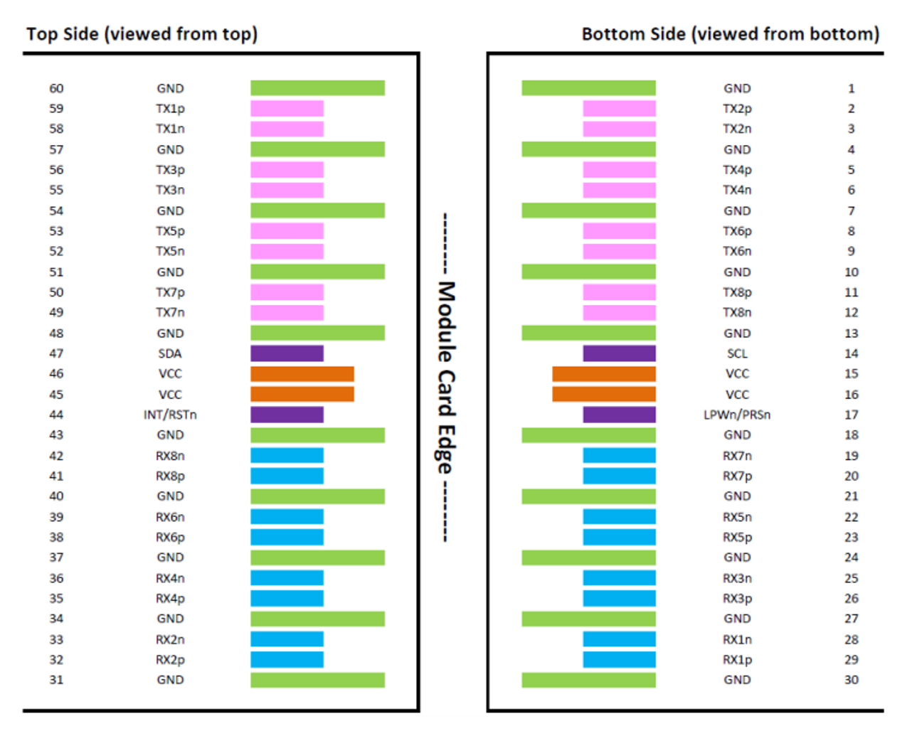
Pin Descriptions
The device is is compliant with the Specification for OSFP (Octal Small Form Factor Pluggable) Modules for the head end (www.osfpmsa.org) and the SFF-8636 specification for the tails (www.snia.org/technology-communities/sff/specifications).
The pin assignment for the interface is shown below.
|
Pin |
Symbol |
Description |
Pin |
Symbol |
Description |
|
1 |
GND |
Ground |
31 |
GND |
Ground |
|
2 |
Tx2p |
Transmitter Non-Inverted Data Input |
32 |
Rx2p |
Receiver Non-Inverted Data Output |
|
3 |
Tx2n |
Transmitter Inverted Data Input |
33 |
Rx2n |
Receiver Inverted Data Output |
|
4 |
GND |
Ground |
34 |
GND |
Grounds |
|
5 |
Tx4p |
Transmitter Non-Inverted Data Input |
35 |
Rx4p |
Receiver Non-Inverted Data Output |
|
6 |
Tx4n |
Transmitter Inverted Data Input |
36 |
Rx4n |
Receiver Inverted Data Output |
|
7 |
GND |
Ground |
37 |
GND |
Ground |
|
8 |
Tx6p |
Transmitter Non-Inverted Data Input |
38 |
Rx6p |
Receiver Non-Inverted Data Output |
|
9 |
Tx6n |
Transmitter Inverted Data Input |
39 |
Rx6n |
Receiver Inverted Data Output |
|
10 |
GND |
Ground |
40 |
GND |
Ground |
|
11 |
Tx8p |
Transmitter Non-Inverted Data Input |
41 |
Rx8p |
Receiver Non-Inverted Data Output |
|
12 |
Tx8n |
Transmitter Inverted Data Input |
42 |
Rx8n |
Receiver Inverted Data Output |
|
13 |
GND |
Ground |
43 |
GND |
Ground |
|
14 |
SCL |
2-wire serial interface clock |
44 |
INT / RSTn |
Module Interrupt / Module Reset |
|
15 |
VCC |
+3.3V Power |
45 |
VCC |
+3.3V Power |
|
16 |
VCC |
+3.3V Power |
46 |
VCC |
+3.3V Power |
|
17 |
LPWn / PRSn |
Low-Power Mode / Module Present |
47 |
SDA |
2-wire Serial interface data |
|
18 |
GND |
Ground |
48 |
GND |
Ground |
|
19 |
Rx7n |
Receiver Inverted Data Output |
49 |
Tx7n |
Transmitter Inverted Data Input |
|
20 |
Rx7p |
Receiver Non-Inverted Data Output |
50 |
Tx7p |
Transmitter Non-Inverted Data Input |
|
21 |
GND |
Ground |
51 |
GND |
Ground |
|
22 |
Rx5n |
Receiver Inverted Data Output |
52 |
Tx5n |
Transmitter Inverted Data Input |
|
23 |
Rx5p |
Receiver Non-Inverted Data Output |
53 |
Tx5p |
Transmitter Non-Inverted Data Input |
|
24 |
GND |
Ground |
54 |
GND |
Ground |
|
25 |
Rx3n |
Receiver Inverted Data Output |
55 |
Tx3n |
Transmitter Inverted Data Input |
|
26 |
Rx3p |
Receiver Non-Inverted Data Output |
56 |
Tx3p |
Transmitter Non-Inverted Data Input |
|
27 |
GND |
Ground |
57 |
GND |
Ground |
|
28 |
Rx1n |
Receiver Inverted Data Output |
58 |
Tx1n |
Transmitter Inverted Data Input |
|
29 |
Rx1p |
Receiver Non-Inverted Data Output |
59 |
Tx1p |
Transmitter Non-Inverted Data Input |
|
30 |
GND |
Ground |
60 |
GND |
Ground |
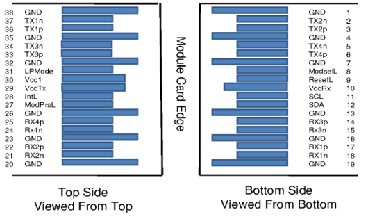
OSFP Module Pad Layout
The MCP7Y60 pin assignment is SFF-8679 compliant for the two 200G ‘tails’ with QSFP56 form factor:
|
Pin |
Symbol |
Description |
Pin |
Symbol |
Description |
|
1 |
Ground |
Ground |
20 |
Ground |
Ground |
|
2 |
Tx2n |
Connected to lane Rx2 |
21 |
Rx2n |
Connected to lane Tx2 |
|
3 |
Tx2p |
Connected to lane Rx2 |
22 |
Rx2p |
Connected to lane Tx2 |
|
4 |
Ground |
Ground |
23 |
Ground |
Grounds |
|
5 |
Not connected |
Not connected |
24 |
Not connected |
Not connected |
|
6 |
Not connected |
Not connected |
25 |
Not connected |
Not connected |
|
7 |
Ground |
Ground |
26 |
Ground |
Ground |
|
8 |
Mod-SelL |
Cable Select |
27 |
ModPrsL |
Cable Present |
|
9 |
ResetL |
Cable Reset |
28 |
IntL |
Interrupt |
|
10 |
Vcc Rx |
+3.3V Power supply receiver |
29 |
Vcc Tx |
+3.3V Power supply transmitter |
|
11 |
SCL |
2-wire serial interface clock |
30 |
Vcc1 |
+3.3V Power Supply |
|
12 |
SDA |
2-wire serial interface data |
31 |
LPMode |
Low Power Mode |
|
13 |
Ground |
Ground |
32 |
Ground |
Ground |
|
14 |
Not connected |
Not connected |
33 |
Not connected |
Not connected |
|
15 |
Not connected |
Not connected |
34 |
Not connected |
Not connected |
|
16 |
Ground |
Ground |
35 |
Ground |
Ground |
|
17 |
Rx1p |
Connected to lane Tx1 |
36 |
Tx1p |
Connected to lane Rx1 |
|
18 |
Rx1n |
Connected to lane Tx1 |
37 |
Tx1n |
Connected to lane Rx1 |
|
19 |
Ground |
Ground |
38 |
Ground |
Ground |
QSFP56 Module Pad Layout