Specifications
Absolute maximum ratings are those beyond which the device may be damaged.
Parameter | Symbol | Min | Max | Unit |
Storage Temperature | TS | -40 | 85 | °C |
Operating Case Temperature | TOP | 0 | 70 | °C |
Power Supply Voltage | VccRx, Vcc1, VccTx | 0 | 3.6 | V |
Relative Humidity (non-condensing) | RH | 5 | 85 | % |
Damage Threshold | THd | 3.0 | --- | dBm |
Parameter | Symbol | Min | Typ | Max | Unit |
Operating Case Temperature | TOP | 0 | --- | 70 | C |
Power Supply Voltage | VccRx, Vcc1, VccTx | 3.135 | 3.3 | 3.465 | V |
Data Rate | --- | -100 ppm | 25.78125 | + 100 ppm | Gbps |
Control Input Voltage High | VCTLH | 2.0 | --- | Vcc | V |
Control Input Voltage Low | VCTLL | 0.0 | --- | 0.8 | V |
Link Distance with ITU-T G.652.D | D | 0.002 | --- | 10 | km |
Parameter | Symbol | Min | Typ | Max | Unit | Note |
Power Consumption | --- | --- | --- | 1.5 | W | |
Transmitter | ||||||
Differential Input Voltage Swing | VIN,PP | 200 | --- | 900 | mVpp | |
Common Mode Voltage | VCM | -350 | --- | 2850 | mV | 1 |
Differential Termination Mismatch | ZIN | --- | --- | 10 | % | At 1 MHz |
Receiver | ||||||
Differential Output Voltage Swing | VOUT,PP | --- | --- | 900 | mVpp | |
Common Mode Voltage | VCM | -350 | --- | 2850 | mV | 1 |
Differential Termination Mismatch | ZIN | --- | --- | 10 | % | At 1 MHz |
Common Mode Return Loss | SCC22 | --- | --- | -2 | dB | 2 |
Transition Time, 20 to 80% | 9.5 | --- | --- | ps | ||
Eye Width at 10-15 probability | EW15 | 0.57 | --- | --- | UI | |
Eye Height at 10-15 probability | EH15 | 228 | --- | --- | mVpp | 3 |
Notes:
VCM is generated by the host. The specification includes effects of ground offset voltage.
From 250 MHz to 30 GHz.
Requires optimization of equalizer/emphasis and de-embedding of test cables to get correct reading.
Power-on Initialization Time is the time from when the supply voltages reach and remain above the minimum specified operating supply voltages to the time when the module is fully function Timing is specified in SFF-8402 [1].
Parameter | Symbol | Min | Typ | Max | Unit | Note |
Wavelength | λ | 1295 | --- | 1325 | nm | |
Transmitter | ||||||
Side Mode Suppression Mode | SMSR | 30 | --- | --- | dB | |
Average Launch Power | PAVG | -7 | 2 | dBm | ||
Optical Modulation Amplitude (OMA) | POMA | -4 | --- | 2.2 | dBm | 1 |
Launch Power in OMA minus Transmitter and Dispersion Penalty (TDP), each Lane | --- | -5 | --- | --- | dBm | |
TDP, each Lane | TDP | --- | --- | 2.7 | dB | |
Extinction Ratio | ER | 3 | --- | --- | dB | |
Relative Intensity Noise | RIN | --- | --- | -130 | dB/Hz | |
Optical Return Loss Tolerance | ORLT | --- | --- | 20 | dB | |
Transmitter Reflectance | TFL | --- | --- | -26 | dB | |
Avg Launch Power, when OFF | POFF | --- | --- | -30 | dBm | |
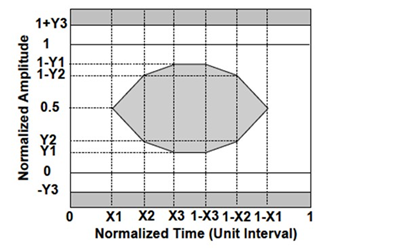
Eye Mask{X1, X2, X3, Y1, Y2, Y3} | {0.31, 0.4, 0.45, 0.34, 0.38, 0.4} | 2 | ||||
Receiver | ||||||
Center Wavelength | λr | 1295 | --- | 1325 | nm | |
Damage Threshold | THd | 3 | --- | --- | dBm | 3 |
Average Receive Power | AOP | --- | --- | 2.2 | dBm | |
Optical Modulation Amplitude | OMA | -14 | --- | 2 | dBm | |
Receiver Sensitivity (OMA) | SEN | --- | --- | -12 | dBm | 2 |
Stressed Receiver Sensitivity (OMA) | --- | --- | -9.5 | dBm | 4 | |
Receiver Reflectance | RR | --- | --- | -26 | dB | |
LOS Assert | LOSA | -30 | --- | dBm | ||
LOS Deassert | LOSD | --- | --- | -15 | dBm | |
LOS Hysteresis | LOSH | 0.5 | --- | --- | dB | |
Receiver Electrical 3 dB upper cutoff frequency | fC | --- | --- | 31 | GHz | |
Conditions of Stressed Receiver Sensitivity Test (Note 5) | ||||||
Vertical Eye Closure Penalty, each lane | --- | --- | 2.5 | --- | dB | |
Stressed Eye J2 Jitter | --- | --- | 0.27 | --- | UI | |
Stressed Eye J4 Jitter | --- | --- | 0.39 | --- | UI | |
SRS Eye Mask Definition {X1, X2, X3, Y1, Y2, Y3} | {0.31, 0.4, 0.45 0.34, 0.38, 0.4} | |||||
Notes:
Even if the TDP < 1 dB, the OMA min must exceed the minimum value specified here. See Eye Mask Definition figure below.
Hit ratio 5x10⁻⁵ per sample.
The receiver shall be able to tolerate, without damage, continuous exposure to a modulated optical input signal having this power level on one lan The receiver does not have to operate correctly at this input power.
Measured with conformance test signal at receiver input for BER = 5x10⁻⁵.
Vertical eye closure penalty, stressed eye J2 jitter, stressed eye J4 jitter, and SRS eye mask definition are test conditions for measuring stressed receiver sensitivity. They are not required characteristics of the receiver.
Eye Mask Definition
The following digital diagnostic characteristics are defined over the normal operating conditions unless otherwise specified.
Optical Module Specifications
Parameter | Symbol | Value | Units | Notes |
Temperature monitor absolute error | DMI_Temp | ±3 | ºC | Over operating temperature range |
Supply voltage monitor absolute error | DMI_VCC | ±0.1 | V | Over full operating range |
Channel RX power monitor absolute error | DMI_RX_Ch | ±2 | dB | 1 |
Channel Bias current monitor | DMI_Ibias_Ch | ±10 | % | |
Channel TX power monitor absolute error | DMI_TX_Ch | ±2 | dB | 1 |
Note 1: Due to measurement accuracy of different single mode fibers, there could be an additional ±1 dB tolerance, or a ±3 dB total tolerance.
This transceiver is specified as ESD threshold 1 kV for high speed data pins and 2 kV for all other electrical input pins, tested per MIL-STD-883, Method 3015.4 /JESD22-A114-A (HBM). However, normal ESD precautions are still required during the handling of this module. This transceiver is shipped in ESD protective packaging. It should be removed from the packaging and handled only in an ESD protected environment.

The following label is applied on the transceiver's backshell:
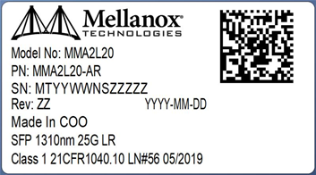
(sample illustration)
Images are for illustration purposes only. Product labels, colors, and lengths may vary.
Transceiver Backshell Label Serial Number Legend
Symbol | Meaning | Notes |
MT | Manufacturer name | 2 digits (alphanumeric) |
YY | Year of manufacturing | 2 last digits of the year (numeric) |
WW | Week of manufacturing | 2 digit (numeric) |
XX | Manufacturer site | Two characters |
SSSSS | Serial number | 5 digits (decimal numeric) for serial number, starting from 00001. |
Safety: The laser module is classified as Class 1 according to EN 60825-1, EN 60950-1, UL60950-1, CAN/CSA-C22.2 60950-1, FDA. This product complies with 21 CFR 1040.10 and 1040.11 except for deviations pursuant to Laser Notice No. 50, dated (June 24, 2007).
EMC: CE, FCC, EN55032 Class A, EN55024, CISPR32 Class A, VCCI Class A.
Telcordia Technologies© GR-468CORE, (shock, vibration, HT operation, damp heat operation).
The following certificates are not available:
Safety: CB
EMC: ICES, RCM
Ask your field engineer or the support team for a zip file of the certifications for this product.
Caution: Use of controls, adjustments or performance of procedures other than those specified herein may result in hazardous radiation exposure.
This device complies with CFR47 FCC Class A Part 15 of the FCC Rules. Operation is subject to the following two conditions:
This device may not cause harmful interference.
This device must accept any interference received, including interference that may cause undesired operation.
Note: This equipment has been tested and found to comply with the limits for a Class A digital device, pursuant to Part 15 of the FCC Rules. These limits are designed to provide reasonable protection against harmful interference in a residential installation. This equipment generates, uses and can radiate radio frequency energy and, if not installed and used in accordance with the instructions, may cause harmful interference to radio communications. However, there is no guarantee that interference will not occur during installation. If this equipment does cause harmful interference to radio or television reception, which can be determined by turning the equipment off and on, the user is encouraged to try to correct the interference by one or more of the following measures:
Reorient or relocate the receiving antenna.
Increase the separation between the equipment and receiver.
Connect the equipment into an outlet on a circuit different from that to which the receiver is connected.
Consult the dealer or an experienced radio/television technician for help.
Modifications: Any modifications made to this device that are not approved by NVIDIA may void the authority granted to the user by the FCC to operate this equipment.