Pin Description
The BF2500 Controller Card uses a PCI Express x16 connector (component and print sides) according to the PCI Express 4.0 specifications. The following two tables provide component side pins description and print side pins description.
|
Pin # |
Signal Name |
I/O |
Description |
Pin # |
Signal Name |
I/O |
Description |
|
A1 |
PRSNT1# |
Input |
Card presence detect, connected to PRSNT2# |
B1 |
12V |
Power |
12V |
|
A2 |
12V |
Power |
12V |
B2 |
12V |
Power |
12V |
|
A3 |
12V |
Power |
12V |
B3 |
12V |
Power |
12V |
|
A4 |
GND |
GND |
Ground |
B4 |
GND |
GND |
Ground |
|
A5 |
TCK |
JTAG - Not Connected |
B5 |
SMCLK |
I/O |
SMBUS_SCL - connected to DPU SoC |
|
|
A6 |
TDI |
Input |
On-board loop |
B6 |
SMDAT |
I/O |
SMBUS_SDA - connected to DPU SoC |
|
A7 |
TDO |
Output |
B7 |
GND |
GND |
Ground |
|
|
A8 |
TMS |
JTAG - Not Connected |
B8 |
3.3V |
Power |
3.3V - Not Connected |
|
|
A9 |
3.3V |
Power |
3.3V - Not Connected |
B9 |
TRST# |
JTAG - Not Connected |
|
|
A10 |
3.3V |
Power |
3.3V - Not Connected |
B10 |
3.3V_AUX |
Power |
3.3V auxiliary power |
|
A11 |
PERST# |
Input |
PCIe Interface Reset#, driven by DPU SoC |
B11 |
WAKE#/RSVD |
Not connected, option connect to NIC_GPIO[13] |
|
|
A12 |
GND |
GND |
Ground |
B12 |
RSVD |
Not connected |
|
|
A13 |
REFCLK+ |
Output |
PCIe Reference Differential Clock. Not connected (default) |
B13 |
GND |
GND |
Ground |
|
A14 |
REFCLK- |
Output |
PCIe Reference Differential Clock. Not connected (default) |
B14 |
PETP0 |
Input |
DPU SoC RX |
|
A15 |
GND |
GND |
Ground |
B15 |
PETN0 |
Input |
DPU SoC RX |
|
A16 |
PERP0 |
Output |
DPU SoC TX |
B16 |
GND |
GND |
Ground |
|
A17 |
PERN0 |
Output |
DPU SoC TX |
B17 |
RSVD |
Ground |
|
|
A18 |
GND |
GND |
Ground |
B18 |
GND |
GND |
Ground |
|
A19 |
RSVD |
Not connected |
B19 |
PETP1 |
Input |
DPU SoC RX |
|
|
A20 |
GND |
GND |
Ground |
B20 |
PETN1 |
Input |
DPU SoC RX |
|
A21 |
PERP1 |
Output |
DPU SoC TX |
B21 |
GND |
GND |
Ground |
|
A22 |
PERN1 |
Output |
DPU SoC TX |
B22 |
GND |
GND |
Ground |
|
A23 |
GND |
GND |
Ground |
B23 |
PETP2 |
Input |
DPU SoC RX |
|
A24 |
GND |
GND |
Ground |
B24 |
PETN2 |
Input |
DPU SoC RX |
|
A25 |
PERP2 |
Output |
DPU SoC TX |
B25 |
GND |
GND |
Ground |
|
A26 |
PERN2 |
Output |
DPU SoC TX |
B26 |
GND |
GND |
Ground |
|
A27 |
GND |
GND |
Ground |
B27 |
PETP3 |
Input |
DPU SoC RX |
|
A28 |
GND |
GND |
Ground |
B28 |
PETN3 |
Input |
DPU SoC RX |
|
A29 |
PERP3 |
Output |
DPU SoC TX |
B29 |
GND |
GND |
Ground |
|
A30 |
PERN3 |
Output |
DPU SoC TX |
B30 |
RSVD |
Not connected |
|
|
A31 |
GND |
GND |
Ground |
B31 |
RSVD |
Not connected |
|
|
A32 |
RSVD |
Not connected |
B32 |
GND |
GND |
Ground |
|
|
A33 |
RSVD |
Not connected |
B33 |
PETP4 |
Input |
DPU SoC RX |
|
|
A34 |
GND |
GND |
Ground |
B34 |
PETN4 |
Input |
DPU SoC RX |
|
A35 |
PERP4 |
Output |
DPU SoC TX |
B35 |
GND |
GND |
Ground |
|
A36 |
PERN4 |
Output |
DPU SoC TX |
B36 |
GND |
GND |
Ground |
|
A37 |
GND |
GND |
Ground |
B37 |
PETP5 |
Input |
DPU SoC RX |
|
A38 |
GND |
GND |
Ground |
B38 |
PETN5 |
Input |
DPU SoC RX |
|
A39 |
PERP5 |
Output |
DPU SoC TX |
B39 |
GND |
GND |
Ground |
|
A40 |
PERN5 |
Output |
DPU SoC TX |
B40 |
GND |
GND |
Ground |
|
A41 |
GND |
GND |
Ground |
B41 |
PETP6 |
Input |
DPU SoC RX |
|
A42 |
GND |
GND |
Ground |
B42 |
PETN6 |
Input |
DPU SoC RX |
|
A43 |
PERP6 |
Output |
DPU SoC TX |
B43 |
GND |
GND |
Ground |
|
A44 |
PERN6 |
Output |
DPU SoC TX |
B44 |
GND |
GND |
Ground |
|
A45 |
GND |
GND |
Ground |
B45 |
PETP7 |
Input |
DPU SoC RX |
|
A46 |
GND |
GND |
Ground |
B46 |
PETN7 |
Input |
DPU SoC RX |
|
A47 |
PERP7 |
Output |
DPU SoC TX |
B47 |
GND |
GND |
Ground |
|
A48 |
PERN7 |
Output |
DPU SoC TX |
B48 |
RSVD |
Not connected |
|
|
A49 |
GND |
GND |
Ground |
B49 |
GND |
GND |
Ground |
|
A50 |
RSVD |
Not connected |
B50 |
PETP8 |
Input |
DPU SoC RX |
|
|
A51 |
GND |
GND |
Ground |
B51 |
PETN8 |
Input |
DPU SoC RX |
|
A52 |
PERP8 |
Output |
DPU SoC TX |
B52 |
GND |
GND |
Ground |
|
A53 |
PERN8 |
Output |
DPU SoC TX |
B53 |
GND |
GND |
Ground |
|
A54 |
GND |
GND |
Ground |
B54 |
PETP9 |
Input |
DPU SoC RX |
|
A55 |
GND |
GND |
Ground |
B55 |
PETN9 |
Input |
DPU SoC RX |
|
A56 |
PERP9 |
Output |
DPU SoC TX |
B56 |
GND |
GND |
Ground |
|
A57 |
PERN9 |
Output |
DPU SoC TX |
B57 |
GND |
GND |
Ground |
|
A58 |
GND |
GND |
Ground |
B58 |
PETP10 |
Input |
DPU SoC RX |
|
A59 |
GND |
GND |
Ground |
B59 |
PETN10 |
Input |
DPU SoC RX |
|
A60 |
PERP10 |
Output |
DPU SoC TX |
B60 |
GND |
GND |
Ground |
|
A61 |
PERN10 |
Output |
DPU SoC TX |
B61 |
GND |
GND |
Ground |
|
A62 |
GND |
GND |
Ground |
B62 |
PETP11 |
Input |
DPU SoC RX |
|
A63 |
GND |
GND |
Ground |
B63 |
PETN11 |
Input |
DPU SoC RX |
|
A64 |
PERP11 |
Output |
DPU SoC TX |
B64 |
GND |
GND |
Ground |
|
A65 |
PERN11 |
Output |
DPU SoC TX |
B65 |
GND |
GND |
Ground |
|
A66 |
GND |
GND |
Ground |
B66 |
PETP12 |
Input |
DPU SoC RX |
|
A67 |
GND |
GND |
Ground |
B67 |
PETN12 |
Input |
DPU SoC RX |
|
A68 |
PERP12 |
Output |
DPU SoC TX |
B68 |
GND |
GND |
Ground |
|
A69 |
PERN12 |
Output |
DPU SoC TX |
B69 |
GND |
GND |
Ground |
|
A70 |
GND |
GND |
Ground |
B70 |
PETP13 |
Input |
DPU SoC RX |
|
A71 |
GND |
GND |
Ground |
B71 |
PETN13 |
Input |
DPU SoC RX |
|
A72 |
PERP13 |
Output |
DPU SoC TX |
B72 |
GND |
GND |
Ground |
|
A73 |
PERN13 |
Output |
DPU SoC TX |
B73 |
GND |
GND |
Ground |
|
A74 |
GND |
GND |
Ground |
B74 |
PETP14 |
Input |
DPU SoC RX |
|
A75 |
GND |
GND |
Ground |
B75 |
PETN14 |
Input |
DPU SoC RX |
|
A76 |
PERP14 |
Output |
DPU SoC TX |
B76 |
GND |
GND |
Ground |
|
A77 |
PERN14 |
Output |
DPU SoC TX |
B77 |
GND |
GND |
Ground |
|
A78 |
GND |
GND |
Ground |
B78 |
PETP15 |
Input |
DPU SoC RX |
|
A79 |
GND |
GND |
Ground |
B79 |
PETN15 |
Input |
DPU SoC RX |
|
A80 |
PERP15 |
Output |
DPU SoC TX |
B80 |
GND |
GND |
Ground |
|
A81 |
PERN15 |
Output |
DPU SoC TX |
B81 |
PRSNT2# |
Output |
x16 PCIe card detection, connected to PRESNT1# |
|
A82 |
GND |
GND |
Ground |
B82 |
RSVD |
Not connected |
Power Sequencing
The BF2500 Controller Card requires the 12V ATX PCIe power to come up prior or at the same time to the +12V at the PCIe edge connector.
|
Pin# |
Signal Name |
I/O |
Description |
Comment |
|
1 |
REF_CLK |
Input |
50M REF CLK for NCSI BUS |
|
|
2 |
GND |
GND |
Ground |
|
|
3 |
ARB_IN |
Input |
NCSI hardware arbitration input |
|
|
4 |
GND |
GND |
Ground |
|
|
5 |
ARB_OUT |
Output |
NCSI hardware arbitration output |
|
|
6 |
GND |
GND |
Ground |
|
|
7 |
RX_D0 |
Output |
Receive data |
Output for SoC |
|
8 |
GND |
GND |
Ground |
|
|
9 |
RX_D1 |
Output |
Receive data |
Output for SoC |
|
10 |
GND |
GND |
Ground |
|
|
11 |
CRS_DV |
Output |
Carrier sense/Receive Data Valid |
|
|
12 |
GND |
GND |
Ground |
|
|
13 |
TX_D0 |
Input |
Transmit data |
Input for SoC |
|
14 |
GND |
GND |
Ground |
|
|
15 |
TX_D1 |
Input |
Transmit data |
Input for SoC |
|
16 |
GND |
GND |
Ground |
|
|
17 |
TX_EN |
Input |
Transmit enable |
|
|
18 |
GND |
GND |
Ground |
|
|
19 |
NC |
|||
|
20 |
NC |
|||
|
21 |
I2C_SDA |
Bidirectional |
I2C Serial Data |
GW_ARM1 |
|
22 |
GND |
GND |
Ground |
|
|
23 |
I2C_SCL |
Bidirectional |
I2C Serial Clock |
GW_ARM1 |
|
24 |
GND |
GND |
Ground |
|
|
25 |
GND |
GND |
Ground |
|
|
26 |
GND |
GND |
Ground |
|
|
27 |
NC |
|||
|
28 |
UART_TX |
Output |
Transmit data |
Output for SoC |
|
29 |
NC |
|||
|
30 |
UART_RX |
Input |
Receive data |
The below table provides the External Power Supply pins of the external power supply interfaces on the DPU. For further details, please refer to External PCIe Power Supply Connector.
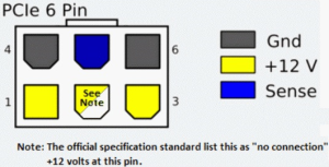
The mechanical pinout of the 6-pin external +12V power connector is shown below. The +12V connector is a GPU power PCIe standard connector. Care should be taken to ensure the power is applied to the correct pins as some 6-pin ATX type connector can have different pinouts.
|
Pin# |
Signal Name |
Description |
|
1 |
12V |
ATX Supplied 12V |
|
2 |
12V |
ATX Supplied 12V |
|
3 |
12V |
ATX Supplied 12V |
|
4 |
GND |
Power Return |
|
5 |
GND |
Power Return |
|
6 |
GND |
Power Return |
External +12V Mechanical Pinout Diagram