Pin Description
PCIe x16 Gen 3.0/4.0 Edge Connector
The BF1600 Controller Card uses a PCI Express x16 connector (component and print sides) according to the PCI Express 3.0/4.0 specifications. The following two tables provide component side pins description and print side pins description. For further details, please refer to PCIe x16 Gen 3.0/4.0 Edge Interface.
HSOp(x) and HSOn(x) stand for High Speed Output and HSIp(x) and HSIn(x) stand for High Speed Input. The direction is relative to the motherboard or system board.
PCIe x16 Edge Connector Pins Description - Print Side
Pin# | Pin Name | Pin Directiona | Description |
1 | PRSNT#1 | Input | The presence detects indication. Should be grounded on the carrier board. |
2 | +12v | Input | Power |
3 | +12v | Input | Power |
4 | GND | Ground | |
5 | JTAG_HOST_TCK | Input | No connected |
6 | JTAG_HOST_TDI | Input | No connected |
7 | JTAG_HOST_TDO | Output | No connected |
8 | JTAG_HOST_TMS | Input | No connected |
9 | +3.3v | Input | Power |
10 | +3.3v | Input | Power |
11 | PERST# | Output | PCIe Interface Reset# For the PCIe interface via the card PCIe Edge connector For System NIC mode, it's direction will turn as input. |
Mechanical Key | |||
12 | GND | Ground | Ground |
13 | REFCLK+ | NA | PCIe Reference Differential Clock. Not Connected (default) Assembly option to support PCIe shared clocking scheme:
|
14 | REFCLK- | ||
15 | GND | Ground | |
16 | HSIp(0) | Output |
|
17 | HSIn(0) | ||
18 | GND | Ground | |
19 | RSVD | NA | NC optional on-board CPLD connectivity |
20 | GND | Ground | |
21 | HSIp(1) | Output |
|
22 | HSIn(1) | ||
23 | GND | Ground | |
24 | GND | Ground | |
25 | HSIp(2) | Output |
|
26 | HSIn(2) | ||
27 | GND | Ground | |
28 | GND | Ground | |
29 | HSIp(3) | Output |
|
30 | HSIn(3) | ||
31 | GND | Ground | |
32 | RSVD | Input | UART0_RXD - Connected to BlueField SoC UART0 RX |
33 | RSVD | Output | UART0_TXD - Connected to BlueField SoC UART0 TX |
34 | GND | Ground | |
35 | HSIp(4) | Output | BlueField Card PCIe TX to Carrier Board PCIe RX |
36 | HSIn(4) | ||
37 | GND | Ground | |
38 | GND | Ground | |
39 | HSIp(5) | Output | BlueField Card PCIe TX to Carrier Board PCIe RX |
40 | HSIn(5) | ||
41 | GND | Ground | |
42 | GND | Ground | |
43 | HSIp(6) | Output | BlueField Card PCIe TX to Carrier Board PCIe RX |
44 | HSIn(6) | ||
45 | GND | Ground | |
46 | GND | Ground | |
47 | HSIp(7) | Output | BlueField Card PCIe TX to Carrier Board PCIe RX |
48 | HSIn(7) | ||
49 | GND | Ground | |
50 | RSVD | NA | Not connected |
51 | GND | Ground | |
52 | HSIp(8) | Output | BlueField Card PCIe TX to Carrier Board PCIe RX |
53 | HSIn(8) | ||
54 | GND | Ground | |
55 | GND | Ground | |
56 | HSIp(9) | Output | BlueField Card PCIe TX to Carrier Board PCIe RX |
57 | HSIn(9) | ||
58 | GND | Ground | |
59 | GND | Ground | |
60 | HSIp(10) | Output | BlueField Card PCIe TX to Carrier Board PCIe RX |
61 | HSIn(10) | ||
62 | GND | Ground | |
63 | GND | Ground | |
64 | HSIp(11) | Output | BlueField Card PCIe TX to Carrier Board PCIe RX |
65 | HSIn(11) | ||
66 | GND | Ground | |
67 | GND | Ground | |
68 | HSIp(12) | Output | BlueField Card PCIe TX to Carrier Board PCIe RX |
69 | HSIn(12) | ||
70 | GND | Ground | |
71 | GND | Ground | |
72 | HSIp(13) | Output | BlueField Card PCIe TX to Carrier Board PCIe RX |
73 | HSIn(13) | ||
74 | GND | Ground | |
75 | GND | Ground | |
76 | HSIp(14) | Output | BlueField Card PCIe TX to Carrier Board PCIe RX |
77 | HSIn(14) | ||
78 | GND | Ground | |
79 | GND | Ground | |
80 | HSIp(15) | Output | BlueField Card PCIe TX to Carrier Board PCIe RX |
81 | HSIn(15) | ||
82 | GND | Ground | |
a. From BlueField BF1600 Controller Card Perspective.
PCIe x16 Edge Connector Pinouts Description - Component Side
Pin# | Name | PCIe Description | Description |
1 | +12v | Input | Power |
2 | +12v | Input | Power |
3 | +12v | Input | Power |
4 | GND | Ground | |
5 | SMCLK | Input | SMBUS_SCL - connected to BlueField SoC SMB2 Inter- face SCL |
6 | SMDAT | bidirectional | SMBUS_SDA - connected to BlueField SoC SMB2 Inter- face SDA |
7 | GND | Ground | |
8 | +3.3v | Input | Power |
9 | JTAG_TRS T# | Input | For testing purposes only. Keep it floating. |
10 | 3.3Vaux | Input | 3.3V_AUX |
11 | WAKE# | NA | Not Connected. Assembly option for on-board CPLD connectivity |
Mechanical Key | |||
12 | RSVD | NA | For testing purposes only. Keep it floating. |
13 | GND | Ground | |
14 | HSOp(0) | Input |
|
15 | HSOn(0) | ||
16 | GND | Ground | |
17 | PRSNT#2 | NA | Not Connected. Assembly option for on-board CPLD connectivity |
18 | GND | Ground | |
19 | HSOp(1) | Input |
|
20 | HSOn(1) | ||
21 | GND | Ground | |
22 | GND | Ground | |
23 | HSOp(2) | Input |
|
24 | HSOn(2) | ||
25 | GND | Ground | |
26 | GND | Ground | |
27 | HSOp(3) | Input |
|
28 | HSOn(3) | ||
29 | GND | Ground | |
30 | RSVD | NA | For testing purposes only. Keep it floating. |
31 | PRSNT#2 | NA | For testing purposes only. Keep it floating. |
32 | GND | Ground | |
33 | HSOp(4) | Input |
|
34 | HSOn(4) | ||
35 | GND | Ground | |
36 | GND | Ground | |
37 | HSOp(5) | Input | BlueField Card PCIe RX to Carrier Board PCIe TX |
38 | HSOn(5) | ||
39 | GND | Ground | |
40 | GND | Ground | |
41 | HSOp(6) | Input |
|
42 | HSOn(6) | ||
43 | GND | Ground | |
44 | GND | Ground | |
45 | HSOp(7) | Input |
|
46 | HSOn(7) | ||
47 | GND | Ground | |
48 | PRSNT#2 | NA | Not Connected. Assembly option for on-board CPLD connectivity |
49 | GND | Ground | |
50 | HSOp(8) | Input | BlueField Card PCIe RX to Carrier Board PCIe TX |
51 | HSOn(8) | ||
52 | GND | Ground | |
53 | GND | Ground | |
54 | HSOp(9) | Input |
|
55 | HSOn(9) | ||
56 | GND | Ground | |
57 | GND | Ground | |
58 | HSOp(10) | Input |
|
59 | HSOn(10) | ||
60 | GND | Ground | |
61 | GND | Ground | |
62 | HSOp(11) | Input |
|
63 | HSOn(11) | ||
64 | GND | Ground | |
65 | GND | Ground | |
66 | HSOp(12) | Input |
|
67 | HSOn(12) | ||
68 | GND | Ground | |
69 | GND | Ground | |
70 | HSOp(13) | Input |
|
71 | HSOn(13) | ||
72 | GND | Ground | |
73 | GND | Ground | |
74 | HSOp(14) | Input |
|
75 | HSOn(14) | ||
76 | GND | Ground | |
77 | GND | Ground | |
78 | HSOp(15) | Input |
|
79 | HSOn(15) | ||
80 | GND | Ground | |
81 | PRSNT#2 | Output | PRSNT#2 - Hot plug present detect |
82 | RSVD | NA | For testing purposes only. Keep it floating. |
PCIe Gen 3.0 through Two CABLINE-CA II PLUS Connectors
The BlueField BF1600 Controller Card uses two x8 CABLINE-CA II PLUS connectors (Component Side and Print Side Connectors) according to the PCI Express 3.0 specifications. The below two tables provide the component side pins description and the print side pins description. For further details, please refer to PCIe Gen 3.0 through Two CABLINE-CA II PLUS Interfaces.
CABLINE-CA II PLUS Connector - Component Side
The below table provides pins description of the CABLINE-CA II PLUS connector mounted on the controller’s component side.
Pin # | Pin Name | Pin Direction | Description |
1 | GND | Ground | |
2 | PCIE_REF- CLK1_P | NA | PCIe Reference Differential Clock. Not Connected (default) Assembly option to support PCIe shared clocking scheme, then:
|
3 | PCIE_REF- CLK1_N | ||
4 | GND | Ground | |
5 | HSO_15N | Input | BlueField Card PCIe RX to Carrier Board PCIe TX |
6 | HSO_15P | ||
7 | GND | Ground | |
8 | HSO_14N |
|
|
9 | HSO_14P | ||
10 | GND | Ground | |
11 | HSO_13N | Input | BlueField Card PCIe RX to Carrier Board PCIe TX |
12 | HSO_13P | ||
13 | GND | Ground | |
14 | HSO_12N | Input |
|
15 | HSO_12P | ||
16 | GND | Ground | |
17 | HSO_11N |
|
|
18 | HSO_11P | ||
19 | GND | Ground | |
20 | HSO_10N | Input | BlueField Card PCIe RX to Carrier Board PCIe TX |
21 | HSO_10P | ||
22 | GND | Ground | |
23 | HSO_9N | Input | BlueField Card PCIe RX to Carrier Board PCIe TX |
24 | HSO_9P | ||
25 | GND | Ground | |
26 | HSO_8N | Input | BlueField Card PCIe RX to Carrier Board PCIe TX |
27 | HSO_8P | ||
28 | GND | Ground | |
29 | HSO_7N | Input | BlueField Card PCIe RX to Carrier Board PCIe TX |
30 | HSO_7P | ||
31 | GND | Ground | |
32 | HSO_6N | Input | BlueField Card PCIe RX to Carrier Board PCIe TX |
33 | HSO_6P | ||
34 | GND | Ground | |
35 | HSO_5N | Input | BlueField Card PCIe RX to Carrier Board PCIe TX |
36 | HSO_5P | ||
37 | GND | Ground | |
38 | HSO_4N | Input | BlueField Card PCIe RX to Carrier Board PCIe TX |
39 | HSO_4P | ||
40 | GND | Ground | |
41 | HSO_3N | Input | BlueField Card PCIe RX to Carrier Board PCIe TX |
42 | HSO_3P | ||
43 | GND | Ground | |
44 | HSO_2N | Input | BlueField Card PCIe RX to Carrier Board PCIe TX |
45 | HSO_2P | ||
46 | GND | Ground | |
47 | HSO_1N | Input | BlueField Card PCIe RX to Carrier Board PCIe TX |
48 | HSO_1P | ||
49 | GND | Ground | |
50 | HSO_0N | Input | BlueField Card PCIe RX to Carrier Board PCIe TX |
51 | HSO_0P | ||
52 | GND | Ground | |
53 | I2C_SMDAT | NA | Not Connected. |
54 | I2C_SMCLK | NA | Not Connected. |
55 | RSVD | NA | Not Connected. |
56 | S_WAKE1_- CONN_L | NA | Not Connected. |
57 | RSVD | NA | Not Connected. |
58 | RSVD | NA | Not Connected. |
59 | S_PRSNT1_L | Input | Presence Indication. |
60 | RSVD | NA | Not Connected. Keep it floating. |
CABLINE-CA II PLUS Connector - Print Side
The below table provides pins description of the CABLINE-CA II PLUS connector mounted on the con- troller’s print side.
Pin # | Pin Name | Pin Direction | Description |
1 | RSVD | NA | Not Connected. Optional assembly connectivity to BlueField SoC UART1 TXD |
2 | RSVD | NA | Not Connected. Optional assembly connectivity to BlueField SoC UART1 RXD |
3 | RSVD | NA | Not Connected. Assembly option for on-board CPLD connectivity |
4 | RSVD | NA | Not Connected. Assembly option for on-board CPLD connectivity |
5 | RSVD | NA | Not Connected. Assembly option for on-board CPLD connectivity |
6 | RSVD | NA | Not Connected. Assembly option for on-board CPLD connectivity |
7 | RSVD | NA | Not Connected. Assembly option for on-board CPLD connectivity |
8 | RSVD | NA | Not Connected. Assembly option for on-board CPLD connectivity |
9 | GND | Ground | |
10 | HSI_0P | Output | BlueField Card PCIE TX to Carrier Board PCIE RX |
11 | HSI_0N | ||
12 | GND | Ground | |
13 | HSI_1P | Output | BlueField Card PCIE TX to Carrier Board PCIE RX |
14 | HSI_1N | ||
15 | GND | Ground | |
16 | HSI_2P | Output | BlueField Card PCIE TX to Carrier Board PCIE RX |
17 | HSI_2N | ||
18 | GND | Ground | |
19 | HSI_3P | Output | BlueField Card PCIE TX to Carrier Board PCIE RX |
20 | HSI_3N | ||
21 | GND | Ground | |
22 | HSI_4P | Output | BlueField Card PCIE TX to Carrier Board PCIE RX |
23 | HSI_4N | ||
24 | GND | Ground | |
25 | HSI_5P | Output | BlueField Card PCIE TX to Carrier Board PCIE RX |
26 | HSI_5N | ||
27 | GND | Ground | |
28 | HSI_6P | Output | BlueField Card PCIE TX to Carrier Board PCIE RX |
29 | HSI_6N | ||
30 | GND | Ground | |
31 | HSI_7P | Output | BlueField Card PCIE TX to Carrier Board PCIE RX |
32 | HSI_7N | ||
33 | GND | Ground | |
34 | HSI_8P | Output | BlueField Card PCIE TX to Carrier Board PCIE RX |
35 | HSI_8N | ||
36 | GND | Ground | |
37 | HSI_9P | Output | BlueField Card PCIE TX to Carrier Board PCIE RX |
38 | HSI_9N | ||
39 | GND | Ground | |
40 | HSI_10P | Output | BlueField Card PCIE TX to Carrier Board PCIE RX |
41 | HSI_10N | ||
42 | GND | Ground | |
43 | HSI_11P | Output | BlueField Card PCIE TX to Carrier Board PCIE RX |
44 | HSI_11N | ||
45 | GND | Ground | |
46 | HSI_12P | Output | BlueField Card PCIE TX to Carrier Board PCIE RX |
47 | HSI_12N | ||
48 | GND | Ground | |
49 | HSI_13P | Output | BlueField Card PCIE TX to Carrier Board PCIE RX |
50 | HSI_13N | ||
51 | GND | Ground | |
52 | HSI_14P | Output | BlueField Card PCIE TX to Carrier Board PCIE RX |
53 | HSI_14N | ||
54 | GND | Ground | |
55 | HSI_15P | Output | BlueField Card PCIE TX to Carrier Board PCIE RX |
56 | HSI_15N | ||
57 | GND | Ground | |
58 | PERST# | Output | PCIe Interface Reset# for the PCIe interface via the card IPEX connectors For System NIC mode, its direction will turn as input. |
59 | RSVD | NA | Not Connected. Keep it floating. |
60 | S_PRSNT2_L | Input | Presence Indication Should be grounded and shorted to IPEX Component Side pin #58. |
Power Sequencing
The BF1600 Controller Card requires the +3.3V to come up prior to the +12V at the PCIe connector.
The below table lists the NCSI Management Interface pins description. For further details, please refer to NCSI Management Interface.
Pin # | Pin Name | Description |
1 | REF_CLK | Clock reference for receive, transmit, and control interface |
2 | GND | Connected to Board Ground |
3 | ARB_IN | Network Controller hardware arbitration Input |
4 | GND | Connected to Board Ground |
5 | ARB_OUT | Network Controller hardware arbitration Output |
6 | GND | Connected to Board Ground |
7 | RXD0 | Receive data |
8 | GND | Connected to Board Ground |
9 | RXD1 | Receive data |
10 | GND | Connected to Board Ground |
11 | CRS_DV | Carrier Sense/Receive Data Valid |
12 | GND | Connected to Board Ground |
13 | TXD0 | Transmit data |
14 | GND | Connected to Board Ground |
15 | TXD1 | Transmit data |
16 | GND | Connected to Board Ground |
17 | TX_EN | Transmit enable |
18 | GND | Connected to Board Ground |
19 | RX_ER | Receive Error, keep float at system side |
20 | GND | Connected to Board Ground |
21 | I2C_SDA | Used for testing. Keep float at system side. |
22 | GND | Connected to Board Ground |
23 | I2C_SCL | Used for testing. Keep float at system side. |
24 | GND | Connected to Board Ground |
25 | GND | Connected to Board Ground |
26 | GND | Connected to Board Ground |
27 | 3.3V_AUX | Used for testing. Keep float at system side. |
28 | 3.3V_AUX | Used for testing. Keep float at system side. |
29 | 3.3V_AUX | Used for testing. Keep float at system side. |
30 | 3.3V_AUX | Used for testing. Keep float at system side. |
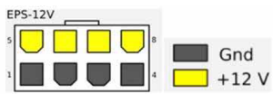
The below table lists the External Power Supply pins of the external power supply interfaces on the BF1600 Controller card and PCIe auxiliary card. For further details, please refer to External PCIe Power Supply Interfaces.
Pin # | Signal Name | Description |
1 | GND | Power Return |
2 | GND | Power Return |
3 | GND | Power Return |
4 | GND | Power Return |
5 | +12V | ATX Supplied 12V |
6 | +12V | ATX Supplied 12V |
7 | +12V | ATX Supplied 12V |
8 | +12V | ATX Supplied 12V |
External +12V Mechanical Pinout Diagram
The below table lists the UART0 interface pins from the BlueField Controller Card perspective. For further details, please refer to UART0 Interface.
The electrical levels of the UART0 interface is CMOS (3.3V)
UART0 Pinouts Description
Pin # | Signal Name |
1 | Receive |
2 | Transmit |
3 | GND |
The below table lists the JTAG CoreSight 10 pins description. For further details, please refer to JTAG CoreSight 10 Interface.
Pin | Signal Name | Voltage Domain | Description |
1 | VTREF | A | The Voltage Target Reference pin supplies DSTREAM with the debug rail voltage of the target to match its I/O logic levels. VTREF can be tied HIGH on the target. If VTREF is pulled HIGH by a resistor, its value must be no greater than 100Ω. |
2 | TMS | A | The Test Mode Select pin sets the state of the Test Access Port (TAP) controller on the target. TMS can be pulled HIGH on the target to keep the TAP controller inactive when not in use. |
3 | GND | NA | Ground. |
4 | TCK | A | The Test Clock pin clocks data into the TDI and TMS inputs of the target. TCK is typically pulled HIGH on the target. |
5 | GND | NA | Ground. |
6 | TDO | A | The Test Data Out pin receives serial data from the target during debugging. You are advised to series terminate TDO close to the target processor. TDO is typically pulled HIGH on the target. |
7 | KEY (NC) | NA | This pin must not be present on the target connector. |
8 | TDI | A | The Test Data In pin provides serial data to the target during debugging. TDI can be pulled HIGH on the target. |
9 | GND | NA | Ground. |
10 | nSRST | A | The System Reset pin fully resets the target. This signal can be initiated by DSTREAM or by the target board (which is then detected by DSTREAM). nSRST is typically pulled HIGH on the target and pulled strong-LOW to initiate a reset. The polarity and strength of nSRST is configurable. |
The below table lists the DDR4 DRAM pins description. For further details, please refer to DDR4 SODIMM Memory.
Pin Name | Description | Pin Name | Description |
A0–A16 | SDRAM address bus | SCL | I2C serial bus clock for SPD/TS |
BA0, BA1 | SDRAM bank select | SDA | I2C serial bus data line for SPD/TS |
BG0, BG1 | SDRAM bank group select | SA0–SA2 | I2C slave address select for SPD/TS |
RAS_na | SDRAM row address strobe | PARITY | SDRAM parity input |
CAS_nb | SDRAM column address strobe | VDD | SDRAM I/O & core power supply |
WE_nc | SDRAM write enable | VPP | SDRAM activating power supply |
CS0_n, CS1_n CS2_n, CS3_n | Rank Select Lines | C0, C1 | Chip ID lines for 3DS components |
CKE0, CKE1 | SDRAM clock enable lines | VREFCA | SDRAM command/address reference supply |
ODT0, ODT1 | SDRAM on-die termination control lines | VSS | Power supply return (ground) |
ACT_n | SDRAM activate | VDDSPD | Serial SPD/TS positive power supply |
DQ0–DQ63 | DIMM memory data bus | ALERT_n | SDRAM ALERT_n |
CB0–CB7 | DIMM ECC check bits | ||
DQS0_t– DQS8_t | SDRAM data strobes (positive line of differential pair) | RESET_n | Set SDRAMs to a Known State |
DQS0_c– DQS8_c | SDRAM data strobes (negative line of differential pair) | EVENT_ n | SPD signals a thermal event has occurred. |
DM0_n–DM8_n, DBI0_n-DBI8_n | SDRAM data masks/data bus inversion (x8-based x72 DIMMs) | VTT | Termination supply for the Address, Command and Control bus |
CK0_t, CK1_t | SDRAM clocks (positive line of differential pair) | NC | No connection |
CK0_c, CK1_c | SDRAM clocks (negative line of differential pair) |
RAS_n is a multiplexed function with A16.
SDRAM column address strobe
WE_n is a multiplexed function with A14.