Specifications
Absolute maximum ratings are those beyond which damage to the device may occur.
Prolonged operation between the operational specifications and absolute maximum ratings is not intended and may cause permanent device degradation.
|
Parameter |
Min |
Max |
Units |
|
Supply voltage |
-0.3 |
3.6 |
V |
|
Data input voltage |
-0.3 |
3.465 |
V |
|
Control input voltage |
-0.3 |
4.0 |
V |
|
Damage threshold |
3.4 |
--- |
dBm |
This table shows the environmental specifications for the product.
|
Parameter |
Min |
Max |
Units |
|
Storage temperature |
-40 |
85 |
°C |
This section shows the range of values for normal operation.
|
Parameter |
Min |
Typ |
Max |
Units |
|
Supply voltage (Vcc) |
3.135 |
3.3 |
3.465 |
V |
|
Power consumption (each end, retiming on all lanes) |
--- |
4.5 |
5.0 |
W |
|
Supply noise tolerance (10Hz – 10MHz) |
66 |
--- |
--- |
mVpp |
|
Operating case temperature |
0 |
--- |
70 |
°C |
|
Operating relative humidity |
5 |
--- |
85 |
% |
|
Parameter |
Min |
Typ |
Max |
Units |
|
Signaling rate |
-100 ppm |
26.5625 |
+100 ppm |
GBd |
|
Differential data input swing at TP1a |
--- |
900 |
mVpp |
|
|
Differential data output swing at TP4 |
--- |
--- |
900 |
mVpp |
|
Near-end ESMW (Eye Symmetry Mask Width) |
0.265 |
--- |
--- |
UI |
|
Near-end output eye height |
70 |
--- |
--- |
mVpp |
|
Output transition time, 20% to 80% |
9.5 |
--- |
--- |
ps |
Notes:
Multiple clock domains are supported only on line-side Rx. Host side Rx supports a single clock domain only.
QSFP Tx CDR lock can only occur if Tx lane 1 is transmitting data.
|
Parameter |
Min |
Typ |
Max |
Units |
|
Transmitter (per lane) |
||||
|
Signaling speed (with retiming) |
-100 ppm |
26.5625 |
+100 ppm |
GBd |
|
Center wavelength |
840 |
850 |
860 |
nm |
|
Spectral width |
--- |
--- |
0.6 |
nm |
|
Average launch power |
-2.0 |
--- |
3.0 |
dBm |
|
Transmit OMA |
-2.0 |
--- |
3.0 |
dBm |
|
Average launch power of off transmitter |
--- |
--- |
-30 |
dBm |
|
Extinction ratio |
4.0 |
--- |
6.0 |
dB |
|
Transmitter reflectance tolerance |
--- |
--- |
-12.0 |
dB |
|
Transmitter return loss |
--- |
--- |
-18.0 |
dB |
|
Transmitter eye mask definition |
--- |
|||
|
Reach on OM3 multi-mode fiber |
70 |
--- |
--- |
m |
|
Reach on OM4 multi-mode fiber |
100 |
--- |
--- |
m |
|
Receiver (per lane) |
||||
|
Signaling speed (with retiming) |
-100 ppm |
26.5625 |
+100 ppm |
GBd |
|
Center wavelength |
840 |
850 |
860 |
nm |
|
Receive damage threshold (AOP) |
5.0 |
--- |
--- |
dBm |
|
Unstressed receiver sensitivity (OMA) at BER = 10-6 |
--- |
--- |
-5.0 |
dBm |
|
Receiver Reflectance |
--- |
--- |
-18.0 |
dB |
|
LOS assert |
--- |
--- |
-14 |
dBm |
|
LOS hysteresis |
0.5 |
--- |
3.0 |
dB |
|
Stressed receiver sensitivity (OMA) at BER = 10-4 |
--- |
--- |
-3.0 |
dBm |
|
Conditions of stressed receiver sensitivity test |
||||
|
SECQ (Stressed Eye Closure) penalty |
--- |
--- |
4.9 |
dB |
|
OMA of each aggressor lane |
--- |
--- |
3.0 |
dB |
|
Stressed eye mask definition |
TBD |
--- |
||
The receiver’s performance may degrade due to overload if the maximum values for AOP or OMA are exceeded. The damage threshold is specified in the Absolute Maximum Ratings table.
The MMA1T00 transceiver supports rate select, which is controlled by writing to registers 0x57-0x58. Two bits are assigned for each receiver lane in byte 0x57 (87dec, Rxn_Rate_Select) and two bits for each transmitter lane in byte 0x58 (88dec, Txn_Rate_Select) to specify up to four bitrates, as defined in SFF-8636 Rev 2.9.2 Table 6-5 XN_RATE_SELECT ENCODINGS. All four lanes are required to have the same rate select value.
The below table specifies the rate for each rate select setting.
Rate Select Encodings
|
Rate Select Value |
Operating Rate (GBd) |
|
10 |
25.78125 NRZ |
|
11 |
26.56250 PAM4 |

The following label is applied on the cable’s backshell:
Backshell Label
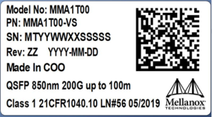
(sample illustration)
Backshell Label Legend
|
Symbol |
Meaning |
Notes |
|
SN – Serial Number |
||
|
MT |
Manufacturer name |
2 characters, e.g. MT |
|
YY |
Year of manufacturing |
2 digits |
|
WW |
Week of manufacturing |
2 digits |
|
XX |
Manufacturer site |
2 characters |
|
SSSSS |
Serial number |
5 digits for serial number, starting from 00001. Reset at start of week to 00001. |
|
Miscellaneous |
||
|
ZZ |
HW and SW revision |
2 alpha-numeric characters |
|
YYYY |
Year of manufacturing |
4 digits |
|
MM |
Month of manufacturing |
2 digits |
|
DD |
Day of manufacturing |
2 digits |
|
COO |
Country of origin |
E.g. China or Malaysia |

|
Quick response code |
Serial number (MTYYWWXXSSSSS) |
The laser module is classified as Class 1 according to IEC 60825-1, IEC 60825-2 and 21 CFR sub J 1040 (CDRH), TÜV/UL60950-1, CAN/CSA-C22.2 60950-1.
EMC: EN55032 Class A, EN55024, AS/NZS CISPR 32 Class A, CISPR32 Class A, VCCI Class A.
Telcordia Technologies© GR-468CORE, (shock, vibration, HT operation, damp heat operation).
Ask your field engineer or NVIDIA support for a zip file of the certifications for this product.
Each of the devices complies with CFR47 FCC Class A Part 15 of the FCC Rules. Operation is subject to the following two conditions:
This device may not cause harmful interference.
This device must accept any interference received, including interference that may cause undesired
Note: This equipment has been tested and found to comply with the limits for a Class A digital device, pursuant to Part 15 of the FCC Rules. These limits are designed to provide reasonable protection against harmful interference in a residential installation. This equipment generates, uses and can radiate radio frequency energy and, if not installed and used in accordance with the instructions, may cause harmful interference to radio communications. However, there is no guarantee that interference will not occur during installation. If this equipment does cause harmful interference to radio or television reception, which can be determined by turning the equipment off and on, the user is encouraged to try to correct the interference by one or more of the following measures:
Reorient or relocate the receiving antenna.
Increase the separation between the equipment and receiver.
Connect the equipment into an outlet on a circuit different from that to which the receiver is connected.
Consult the dealer or an experienced radio/television technician for help.
Modifications: Any modifications made to this device that are not approved by NVIDIA may void the authority granted to the user by the FCC to operate this equipment.