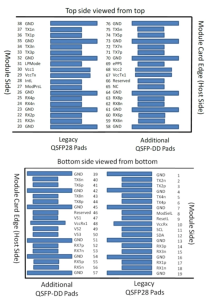
Pin Description
The transceiver’s pin assignment is SFF-8679 compliant.
|
Pin |
Symbol |
Description |
Pin |
Symbol |
Description |
|
1 |
GND |
Ground |
39 |
GND |
Ground |
|
2 |
Tx2n |
Transmitter Inverted Data Input |
40 |
Tx6n |
Transmitter Inverted Data Input |
|
3 |
Tx2p |
Transmitter Non-Inverted Data Input |
41 |
Tx6p |
Transmitter Non-Inverted Data Input |
|
4 |
GND |
Ground |
42 |
GND |
Ground |
|
5 |
Tx4n |
Transmitter Inverted Data Input |
43 |
Tx8n |
Transmitter Inverted Data Input |
|
6 |
Tx4p |
Transmitter Non-Inverted Data Input |
44 |
Tx8p |
Transmitter Non-Inverted Data Input |
|
7 |
GND |
Ground |
45 |
GND |
Ground |
|
8 |
ModSelL |
Module Select |
46 |
Reserved |
For future use |
|
9 |
ResetL |
Module Reset |
47 |
VS1 |
Module Vendor Specific 1 |
|
10 |
Vcc Rx |
+3.3V Power Supply Receiver |
48 |
VccRx1 |
3.3V Power Supply |
|
11 |
SCL |
2-wire Serial Interface Clock |
49 |
VS2 |
Module Vendor Specific 2 |
|
12 |
SDA |
2-wire Serial Interface Data |
50 |
VS3 |
Module Vendor Specific 3 |
|
13 |
GND |
GND |
51 |
GND |
Ground |
|
14 |
Rx3p |
Receiver Non-Inverted Data Output |
52 |
Rx7p |
Receiver Non-Inverted Data Output |
|
15 |
Rx3n |
Receiver Inverted Data Output |
53 |
Rx7n |
Receiver Inverted Data Output |
|
16 |
GND |
Ground |
54 |
GND |
Ground |
|
17 |
Rx1p |
Receiver Non-Inverted Data Output |
55 |
Rx5p |
Receiver Non-Inverted Data Output |
|
18 |
Rx1n |
Receiver Inverted Data Output |
56 |
Rx5n |
Receiver Inverted Data Output |
|
19 |
GND |
Ground |
57 |
GND |
Ground |
|
20 |
GND |
Ground |
58 |
GND |
Ground |
|
21 |
Rx2n |
Receiver Inverted Data Output |
59 |
Rx6n |
Receiver Inverted Data Output |
|
22 |
Rx2p |
Receiver Non-Inverted Data Output |
60 |
Rx6p |
Receiver Non-Inverted Data Output |
|
23 |
GND |
Grounds |
61 |
GND |
Ground |
|
24 |
Rx4n |
Receiver Inverted Data Output |
62 |
Rx8n |
Receiver Inverted Data Output |
|
25 |
Rx4p |
Receiver Non-Inverted Data Output |
63 |
Rx8p |
Receiver Non-Inverted Data Output |
|
26 |
GND |
Ground |
64 |
GND |
Ground |
|
27 |
ModPrsL |
Module Present |
65 |
NC |
No Connect |
|
28 |
IntL |
Interrupt |
66 |
Reserved |
For future use |
|
29 |
Vcc Tx |
+3.3V Power Supply Transmitter |
67 |
VccTx1 |
3.3V Power Supply |
|
30 |
Vcc1 |
+3.3V Power Supply |
68 |
Vcc2 |
3.3V Power Supply |
|
31 |
LPMode |
Low Power Mode |
69 |
Reserved |
For Future Use |
|
32 |
GND |
Ground |
70 |
GND |
Ground |
|
33 |
Tx3p |
Transmitter Non-Inverted Data Input |
71 |
Tx7p |
Transmitter Non-Inverted Data Input |
|
34 |
Tx3n |
Transmitter Inverted Data Input |
72 |
Tx7n |
Transmitter Inverted Data Input |
|
35 |
GND |
Ground |
73 |
GND |
Ground |
|
36 |
Tx1p |
Transmitter Non-Inverted Data Input |
74 |
Tx5p |
Transmitter Non-Inverted Data Input |
|
37 |
Tx1n |
Transmitter Inverted Data Input |
75 |
Tx5n |
Transmitter Inverted Data Input |
|
38 |
GND |
Ground |
76 |
GND |
Ground |
Notes:
GND is the symbol for signal and supply (power) common for the QSFP modules. All are common within the module and all module voltages are referenced to this potential unless otherwise noted. Connect these directly to the host board signal common ground plane.
VccRx, Vcc1 and VccTx are the receiving and transmission power suppliers and shall be applied concurrently. Recommended host board power supply filtering see SFF-8679.
Pin definitions of the module high speed inputs/outputs
Active fiber ports in MPO12 connector on module side
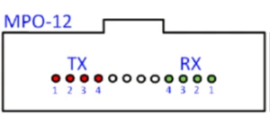
Note: For best performance and least amount of reflections use the angle-polished connector (APC) type.
This transceiver is CMIS 4.0 compliant. The control signals shown in the pad layout are implemented with the following functions:
|
Name |
Function |
Description |
|
ModPrsL |
Output, asserted low |
Pull-up by host when no transceiver/cable is present. Connected to ground inside the transceiver. Hence, asserted low when a transceiver/cable is plugged in. |
|
ModSelL |
Input, asserted Low |
Module Select input pin, terminated high in the module. Only when held low by the host, the module responds to 2-wire serial communication commands. The ModSelL enables multiple modules to share a single 2-wire interface bus. |
|
ResetL |
Input, asserted Low |
Reset input pin, pulled high in the module. A low level on the ResetL pin for longer than the minimum length initiates a module reset. When de-asserted the transceiver starts its initialization procedure. See the CMIS specification [1] for details. |
|
LPMode |
Input, asserted high |
Low Power Mode input, pulled up inside the module. Hardware control signal for forcing the transceiver into low-power state. Can be overwritten by low-power mode command. |
|
ePPS |
Input |
not implemented |
|
IntL |
Output, asserted low |
Interrupt Low is an open-collector output, terminated high in the host system. A “Low” indicates a possible module operational fault or a status critical to the host system, e.g. temperature alarm. The host identifies the source of the interrupt using the 2-wire serial interface. |
The transceiver complies with the SFF-8665 specification and has the following key features:
Physical layer link optimization:
Programmable Tx input equalization
Programmable Rx output amplitude
Programmable Rx output pre-emphasis
Tx/Rx CDR control
by default enabled for 200 Gb/s operation.
Digital Diagnostic Monitoring (DDM):
Rx receive optical power monitor for each lane
Tx transmit optical power monitor for each lane
Tx bias current monitor for each lane
Supply voltage monitor
Transceiver case temperature monitor
Warning and Alarm thresholds for each DDM function (not user changeable)
Other SFF-8636 functions and interrupt indications:
Tx & Rx LOS indication
Tx & Rx LOL indication
Tx fault indication
LOS, LOL, and Tx Fault status flags can be read via the two-wire management interface and are jointly transmitted via the IntL output pin. Relevant advertisement, threshold, and readout registers are found in the CMIS 4.0 MSA.
The transceiver can be damaged by exposure to current surges and over voltage events. Take care to restrict exposure to the conditions defined in Absolute Maximum Ratings. Observe normal handling precautions for electrostatic discharge-sensitive devices. The transceiver is shipped with dust caps on both the electrical and the optical port. The cap on the optical port should always be in place when there is no fiber cable connected. The optical connector has a recessed connector surface which is exposed whenever it has no cable nor cap. Prior to insertion of the fiber cable, clean the cable connector to prevent contamination from it. The dust cap ensures that the optics remain clean, and no additional cleaning should be needed. In the event of contamination, standard cleaning tools and methods should be used. Liquids must not be applied.