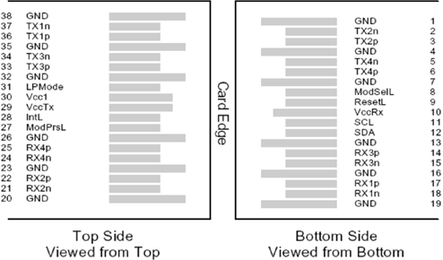
Pin Description
The transceiver’s pin assignment is SFF-8679 compliant.
|
Pin |
Symbol |
Description |
Pin |
Symbol |
Description |
|
1 |
GND |
Ground |
20 |
GND |
Ground |
|
2 |
Tx2n |
Transmitter Inverted Data Input |
21 |
Rx2n |
Receiver Inverted Data Output |
|
3 |
Tx2p |
Transmitter Non-Inverted Data Input |
22 |
Rx2p |
Receiver Non-Inverted Data Output |
|
4 |
GND |
Ground |
23 |
GND |
Ground |
|
5 |
Tx4n |
Transmitter Inverted Data Input |
24 |
Rx4n |
Receiver Inverted Data Output |
|
6 |
Tx4p |
Transmitter Non-Inverted Data Input |
25 |
Rx4p |
Receiver Non-Inverted Data Output |
|
7 |
GND |
Ground |
26 |
GND |
Ground |
|
8 |
ModSelL |
Module Select |
27 |
ModPrsL |
Module Present |
|
9 |
ResetL |
Module Reset |
28 |
IntL |
Interrupt |
|
10 |
Vcc Rx |
+3.3 V Power supply receiver |
29 |
Vcc Tx |
+3.3 V Power supply transmitter |
|
11 |
SCL |
2-wire serial interface clock |
30 |
Vcc1 |
+3.3 V Power Supply |
|
12 |
SDA |
2-wire serial interface data |
31 |
LPMode |
Low Power Mode |
|
13 |
GND |
Ground |
32 |
GND |
Ground |
|
14 |
Rx3p |
Receiver Non-Inverted Data Output |
33 |
Tx3p |
Transmitter Non-Inverted Data Input |
|
15 |
Rx3n |
Receiver Inverted Data Output |
34 |
Tx3n |
Transmitter Inverted Data Input |
|
16 |
GND |
Ground |
35 |
GND |
Ground |
|
17 |
Rx1p |
Receiver Non-Inverted Data Output |
36 |
Tx1p |
Transmitter Non-Inverted Data Input |
|
18 |
Rx1n |
Receiver Inverted Data Output |
37 |
Tx1n |
Transmitter Inverted Data Input |
|
19 |
GND |
Ground |
38 |
GND |
Ground |
QSFP56 Module Pad Layout
This head end of the MCP7F60 is QSFP-Double Density and QSFP56 and the ‘tails’ are QSFP56. This means that the control signals shown in the pad layout and the pin assignments have the following functions:
|
Name |
Function |
Description |
|
ModPrsL |
Output, asserted low |
Pull-up by host when no transceiver/cable is present. Connected to ground inside the transceiver. Hence, asserted low when a transceiver/cable is plugged in. |
|
ModSelL |
Input, asserted Low |
Module Select input pin, terminated high in the module. Only when held low by the host, the module responds to 2-wire serial communication commands. The ModSelL enables multiple modules to share a single 2-wire interface bus. |
|
ResetL |
Input, asserted Low |
Reset input pin, pulled high in the module. A low level on the ResetL pin for longer than the minimum length initiates a module reset. When de-asserted the transceiver starts its initialization procedure. See the CMIS specification. |
|
LPMode |
Input, asserted high |
Low Power Mode input, pulled up inside the module. Hardware control signal for forcing the transceiver into low-power state. Can be overwritten by low-power mode command. |
|
IntL |
Output, asserted low |
Interrupt Low is an open-collector output, terminated high in the host system. A “Low” indicates a possible module operational fault or a status critical to the host system, e.g. temperature alarm. The host identifies the source of the interrupt using the 2-wire serial interface. |
The transceiver complies with the SFF-8665 specification and has the following key features:
Physical layer link optimization:
Programmable Tx input equalization
Programmable Rx output amplitude
Programmable Rx output pre-emphasis
Tx/Rx CDR control
by default enabled for 200 Gb/s operation.
Digital Diagnostic Monitoring (DDM):
Rx receive optical power monitor for each lane
Tx transmit optical power monitor for each lane
Tx bias current monitor for each lane
Supply voltage monitor
Transceiver case temperature monitor
Warning and Alarm thresholds for each DDM function (not user changeable)
Other SFF-8636 functions and interrupt indications:
Tx & Rx LOS indication
Tx & Rx LOL indication
Tx fault indication
LOS, LOL, and Tx Fault status flags can be read via the two-wire management interface and are jointly transmitted via the IntL output pin. Relevant advertisement, threshold, and readout registers are found in the CMIS 4.0 MSA.