Specifications
Absolute maximum ratings are those beyond which damage to the device may occur.
Prolonged operation between the operational specifications and absolute maximum ratings is not intended and may cause permanent device degradation.
|
Parameter |
Symbol |
Min |
Max |
Units |
|
Storage Temperature |
TS |
-40 |
85 |
°C |
|
Relative Humidity (non-condensing) |
RH |
15 |
85 |
% |
|
Supply Voltage |
Vcc |
-0.5 |
3.6 |
V |
This section shows the range of values for normal operation.
|
Parameter |
Symbol |
Min |
Typ |
Max |
Units |
|
Operating temperature (Case) |
TC |
0 |
-- |
70 |
°C |
|
Bit Rate (all wavelengths combined) |
BR |
212.5 |
Gb/s |
||
|
Bit Error Ratio |
BER |
2.4x10⁻⁴ |
|||
|
Reach on SMF OS1 fiber per G.652 |
Lmax (OS1) |
-- |
1000 |
m |
|
|
Reach on SMF OS2 fiber per G.652 |
Lmax (OS2) |
-- |
2000 |
m |
|
Parameter |
Symbol |
Min |
Typical |
Max |
Units |
Notes |
|
Power consumption |
PD |
--- |
--- |
5.5 |
W |
|
|
Transmitter (each lane) |
||||||
|
Signaling rate per lane |
26.5625± 100 ppm. |
Gbd |
||||
|
Differential data input voltage per lane |
Vin,pp,diff |
900 |
mV |
|||
|
Differential termination mismatch |
10 |
% |
||||
|
Single-ended voltage tolerance range |
-0.4 |
3.3 |
V |
|||
|
DC common mode voltage |
|
-350 |
2850 |
mV |
1 |
|
|
Receiver (each lane) |
||||||
|
Signaling rate per lane |
26.5625± 100 ppm. |
Gbd |
||||
|
AC common-mode output voltage (RMS) |
17.5 |
mV |
||||
|
Differential output voltage |
900 |
mV |
||||
|
Near-end ESMW (Eye symmetry mask width) |
0.265 |
UI |
||||
|
Near-end Eye height, differential (min) |
70 |
mV |
||||
|
Far-end ESMW (Eye symmetry mask width) |
0.2 |
UI |
||||
|
Far-end Eye height, differential (min) |
30 |
mV |
||||
|
Far-end pre-cursor ISI ratio |
-4.5 |
2.5 |
% |
|||
|
Differential termination mismatch |
10 |
% |
||||
|
Transition time (min, 20% to 80%) |
9.5 |
ps |
||||
|
DC common mode voltage (min) |
-350 |
2850 |
mV |
1 |
||
Notes:
DC common mode voltage generated by the host. Specification includes effects of ground offset voltage.
|
Parameter |
Min |
Typical |
Max |
Unit |
Notes |
|
|
Transmitter |
||||||
|
Signaling rate (each lane (range) |
26.5625 ± 100 ppm |
GBd |
||||
|
Modulation format |
PAM4 |
|||||
|
Lane wavelength (range) |
1264.5 1284.5 1304.5 1324.5 |
1271 1291 1311 1331 |
1277.5 1297.5 1317.5 1337.5 |
nm |
||
|
Side-mode suppression ratio (SMSR) |
30 |
dB |
||||
|
Total average launch power |
10.7 |
dBm |
||||
|
Average launch power, each lane |
4.7 |
dBm |
||||
|
Average launch power, each lane |
-4.2 |
dBm |
1 |
|||
|
Difference in launch power between any two lanes (OMAouter) max |
4 |
dB |
||||
|
Outer Optical Modulation Amplitude (OMAouter), each lane |
-1.2 |
4.5 |
dBm |
2 |
||
|
Launch power in OMAouter minus TDECQ, each lane |
-2.5 |
dBm |
||||
|
Transmitter and dispersion eye closure for PAM4 (TDECQ), each lane |
3.3 |
dB |
||||
|
Average launch power of OFF transmitter, each lane |
-30 |
dBm |
||||
|
Extinction ratio |
3.5 |
dB |
||||
|
RIN17.1OMA |
-132 |
dB/Hz |
||||
|
Optical return loss tolerance |
17.1 |
dB |
||||
|
Transmitter reflectance |
-26 |
dB |
3 |
|||
|
Receiver |
||||||
|
Signaling rate (each lane (range) |
26.5625 ± 100 ppm |
GBd |
||||
|
Modulation format |
PAM4 |
|||||
|
Lane wavelength (range) |
1264.5 1284.5 1304.5 1324.5 |
1271 1291 1311 1331 |
1277.5 1297.5 1317.5 1337.5 |
nm |
||
|
Damage threshold, each lane |
5.7 |
dBm |
4 |
|||
|
Average receive power, each lane |
4.7 |
dBm |
||||
|
Average receive power, each lane |
-8.2 |
dBm |
5 |
|||
|
Difference in receive power between any two lanes (OMAouter) |
4.1 |
dB |
||||
|
Receiver reflectance |
-26 |
dB |
||||
|
Receiver sensitivity (OMAouter), each lane |
-6.5 |
dBm |
6 |
|||
|
Stressed receiver sensitivity (OMAouter), each lane |
-3.6 |
dBm |
||||
|
Conditions of stressed receiver sensitivity test: (note 5) |
||||||
|
Stressed eye closure for PAM4 (SECQ), lane under test |
3.3 |
dB |
||||
|
OMAouter of each aggressor lane |
0.5 |
dBm |
||||
|
LOS De-Assert |
-9 |
dBm |
||||
|
LOS Assert |
-22 |
-12 |
dBm |
|||
|
LOS Hysteresis |
0.5 |
dB |
||||
Notes:
Average launch power, each lane (min) is informative and not the principal indicator of signal strength. A transmitter with launch power below this value cannot be compliant; however, a value above this does not ensure compliance.
Even if the TDECQ < 1.4 dB for an extinction ratio of 4.5 dB or TDECQ < 1.3 dB for an extinction ratio of < 4.5 dB, the OMAouter (min) must exceed this value.
Transmitter reflectance is defined looking into the transmitter
The receiver shall be able to tolerate, without damage, continuous exposure to an optical input signal having this average power level
Average receive power, each lane (min) is informative and not the principal indicator of signal strength. A received power below this value cannot be compliant; however, a value above this does not ensure compliance.
Receiver sensitivity (OMAouter), each lane (max) is informative and is defined for a transmitter with SECQ up to 1.4 dB.
These test conditions are for measuring stressed receiver sensitivity. They are not characteristics of the receiver.
The transceiver’s register map is accessible as specified in CMIS 4.0 and provides information about connector type, maximum data rate, power class, part number, etc.

The following label is applied on the cable’s backshell:
Backshell Label
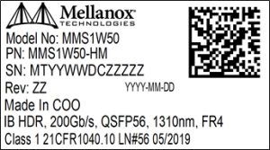
(sample illustration)
Backshell Label Legend
|
Symbol |
Meaning |
Notes |
|
SN – Serial Number |
||
|
MT |
Manufacturer name |
2 characters, e.g. MT |
|
YY |
Year of manufacturing |
2 digits |
|
WW |
Week of manufacturing |
2 digits |
|
XX |
Manufacturer site |
2 characters |
|
SSSSS |
Serial number |
5 digits for serial number, starting from 00001. Reset at start of week to 00001. |
|
Miscellaneous |
||
|
ZZ |
HW and SW revision |
2 alpha-numeric characters |
|
YYYY |
Year of manufacturing |
4 digits |
|
MM |
Month of manufacturing |
2 digits |
|
DD |
Day of manufacturing |
2 digits |
|
COO |
Country of origin |
E.g. China or Malaysia |

|
Quick response code |
Serial number (MTYYWWXXSSSSS) |
The transceiver is a Class 1 laser product. It is certified per the following standards:
|
Feature |
Agency |
Standard |
|
Laser Eye Safety |
FDA/CDRH TÜV |
CDRH 21 CFR 1040 EN60950:2006 +A11+A1+A12+A2, EN60825-1:2014, EN60825-2:2004+A1+A2 |
|
Electrical Safety |
TÜV UL |
IEC 60950-1:2005+A1+A2 UL60950-1 (E243407) |
|
EMC |
Dekra Dekra Dekra ACMA NVIDIA |
AS/NZS CISPR 32: 2013, Class A, EN55032:2012+AC:2013, Class B FCC CFR Title 47 Part 15 Subpart B: 2015, Class B CISPR 22: 2008, ANSI C63.4: 2014 ICES-003 Issue 6: 2016, Class B EN55024:2010+A1 VCCI Class B AS/NZS CISPR 32: 2013, Class A EN 55032:2012/AC2013, Class B, EN 55024:2010 |
|
Electrostatic Discharge to the Receptacle (ESD) |
TÜV |
IEC 61000-4-2 |
|
Robustness |
NVIDIA's CM |
Telcordia GR468 |
|
Environmental |
EN50581: 2012 Hazardous substances REGULATION (EC) NO 1907/2006 (REACH) DIRECTIVE 2011/65/EU (2011/65/EU RoHS recast) |
All versions of this laser are Class 1 laser products per IEC1/EN2 60825-1. Users should observe safety precautions such as those recommended by ANSI3 Z136.1, ANSI Z36.2 and IEC 60825-1.
Each of the devices complies with CFR47 FCC Class A Part 15 of the FCC Rules. Operation is subject to the following two conditions:
This device may not cause harmful interference.
This device must accept any interference received, including interference that may cause undesired
Note: This equipment has been tested and found to comply with the limits for a Class A digital device, pursuant to Part 15 of the FCC Rules. These limits are designed to provide reasonable protection against harmful interference in a residential installation. This equipment generates, uses and can radiate radio frequency energy and, if not installed and used in accordance with the instructions, may cause harmful interference to radio communications. However, there is no guarantee that interference will not occur during installation. If this equipment does cause harmful interference to radio or television reception, which can be determined by turning the equipment off and on, the user is encouraged to try to correct the interference by one or more of the following measures:
Reorient or relocate the receiving antenna.
Increase the separation between the equipment and receiver.
Connect the equipment into an outlet on a circuit different from that to which the receiver is connected.
Consult the dealer or an experienced radio/television technician for help.
Modifications: Any modifications made to this device that are not approved by NVIDIA may void the authority granted to the user by the FCC to operate this equipment.