Overview
The Nvidia Holoscan Sensor Bridge FPGA IP pairs with the Holoscan software and delivers to the end user a sensor-agnostic data-to-ethernet host platform. This IP simplifies and accelerates the FPGA design and can be scaled and configured to adapt to various sensor-to-host applications.
Major functions of the Holoscan Sensor Bridge IP include:
Encapsulate sensor AXI-Stream data into ethernet UDP AXI-Stream data for host processing.
Perform BOOTP, ICMP, and Nvidia defined Ethernet Control Bus (ECB) Networking Protocols.
Transmit enumeration packets and control event packets for pre-defined conditions.
Control peripheral interfaces, such as SPI/I2C/GPIO, to configure sensors and other on-board components.
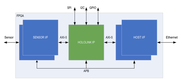
The block diagram of the Holoscan Sensor Bridge IP in the FPGA is depicted below. The Sensor Interface and Host (Ethernet) Interface blocks are FPGA vendor specific logic.

Figure 1. Holoscan Sensor Bridge IP in FPGA
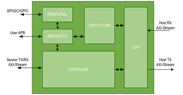
The architecture of the Holoscan Sensor Bridge IP is depicted below.

Figure 2. Holoscan Sensor Bridge IP Architecture
There are 2 main planes of data bridging in the Holoscan Sensor Bridge IP, the Dataplane and the Controlplane. The Dataplane is data transfer relevant to sensor data as it gets packetized to UDP packets. The Controlplane is data transfer relevant to host control. The Controlplane could be receiving and decoding UDP packets from the host to access a register or transmitting specific network protocols the Holoscan Sensor Bridge IP supports.
Resource utilization of the Holoscan Sensor Bridge IP can be provided upon request.