Peripheral Interface
The Holoscan Sensor Bridge IP supports several software defined peripheral interfaces; SPI, I2C and GPIO. For each of these protocols a general-purpose core has been defined to handle all protocol specific requirements and allows for software to set up transactions which are then executed by the Holoscan Sensor Bridge IP.
Multiple endpoints can be supported using one single core instance. In this case, each endpoint will get its own virtual register range, which all map to the same peripheral core instance. The upper bits of this register range act as the MUX select bit to select between the different endpoints. This reduces the overall resource utilization by not requiring multiple instances of the given core. However, this creates the requirement that only one transaction can be set up and executed at a time per protocol, since all endpoints share the same physical registers.
The SPI core is controlled by a series of registers. All SPI transactions are set up through ECB write packets. This system allows software to load a series of data bytes into a buffer, which are then written out to the SPI peripheral. Any data coming from the SPI peripheral will be stored into the same buffer which can then be read through ECB reads.
The SPI core has a 4-bit bi-directional signal data signal (SDIO), a chip select (CS_N) and clock signal (SCK) for each endpoint connected. The bi-directional data signal is broken up into a 4-bit input and 4-bit output signal, with an output enable (oen) signal for tri-stating. This SPI core supports single SPI mode using SDIO[0] as an output (MOSI) and SDIO[1] as an input (MISO). Dual and Quad SPI are supported using 2 and 4 bits of the SDIO signal respectively.
The SPI core is clocked using the i_apb_clk and reset with i_apb_rst. All logic is based off of this clock. For setting the SPI interface’s SCK frequency, a prescaler register is included to divide this clock to slower frequencies. The top-level input should be synchronized to this clock domain. The following code snippets demonstrate how to connect the Holoscan Sensor Bridge SPI interface to top level ports, where “i” is the endpoint index. SPI_SCK, SPI_CSN, SPI_MOSI, SPI_MISO, and SPI_SDIO are top level ports.
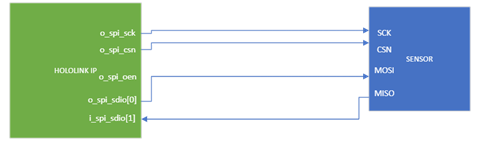
Figure 1. Simple SPI Connectivity
            assign SPI_SCK = o_spi_sck [i];
assign SPI_CSN = o_spi_csn [i];
assign SPI_MOSI = o_spi_sdio [i];
assign i_spi_sdio[i] = {2'b0, SPI_MISO, 1'b0};
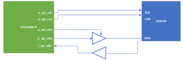
Figure 2. Dual/Quad SPI Connectivity
Dual SPI Assignment
            assign SPI_SCK = o_spi_sck [i];
assign SPI_CSN = o_spi_csn [i];
assign SPI_SDIO [1:0] = o_spi_oen [i] ? o_spi_sdio[i][1:0] : 2'bz;
assign i_spi_sdio [i] = {2’b0,SPI_SDIO};
Quad SPI Assignment
            assign SPI_SCK = o_spi_sck [i];
assign SPI_CSN = o_spi_csn [i];
assign SPI_SDIO = o_spi_oen [i] ? o_spi_sdio[i] : 4'bz;
assign i_spi_sdio [i] = SPI_SDIO;
The I2C CTRL FSM controls the I2C core by a series of registers. All I2C transactions are set up through ECB control packets. This core works in much the same way as the SPI core, where software fills a buffer of data to be written over I2C, and the core handles the protocol-specific handshakes. The I2C core has two bidirectional signals, sda and scl. The core implements this bidirectional signal using an input signal, and an output enable signal. When the output enable signal is high, the corresponding signal should be left floating, only when output enable is low should the output be pulled low. This behavior is consistent with the I2C protocol.
The I2C core is clocked using the i_apb_clk and reset with i_apb_rst. All logic is based off of this clock. For setting the I2C interface’s frequency, a prescaler register is included to divide this clock to slower frequencies.
The top-level input should be synchronized to this clock domain, and glitch filtering should also be added according to the I2C protocol.
The following code snippet demonstrates how to connect the Holoscan Sensor Bridge I2C interface to top level ports, where “i” is the endpoint index. I2C_SCL and I2C_SDA are top level ports.
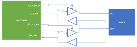
Figure 3. I2C Connectivity
I2C Assignment
            assign i_i2c_scl[i] = o_i2c_scl_en[i] ? I2C_SCL : 1'b0;
assign i_i2c_sda[i] = o_i2c_sda_en[i] ? I2C_SDA : 1'b0;
assign I2C_SCL = o_i2c_scl_en[i] ? 1'bz : 1'b0;
assign I2C_SDA = o_i2c_sda_en[i] ? 1'bz : 1'b0;
*Note: I2C is only verified and tested at 400kHz speed mode.
The Holoscan Sensor Bridge IP supports General Purpose I/O (GPIO) signals for status and control functionality. The GPIO control and status signals can be set or read using ECB write or read.
The GPIO signals can connect to internal user logic or to the top level onto the board. Examples for GPIO control are toggling on-board pins, internal straps to IP configuration, LED control, and more.
Examples for GPIO status are sensor status signals, on-board and internal calibration done signal, software reset count, and more.
GPIO input signals will cross domain clock (CDC) into “i_apb_clk” clock domain.
GPIO output signals will cross domain clock (CDC) into “i_hif_clk” clock domain.
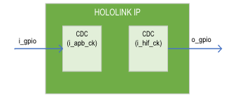
Figure 4. GPIO Connectivity