

MIPI CPNX Reference Design
For developers and sensor module manufacturers focused on building HSB-compatible cameras, radars or other MIPI/GMSL-interfaced sensors, the open-source MIPI CPNX Reference Design is a great launchpad for your project. The FPGA reference design features:
- One or two MIPI interfaces
- Dedicated I2C interfaces for sensor, I2C EEPROM, and auxiliary use.
This design targets the Lattice Semiconductor CertusPro-NX.
Design Overview
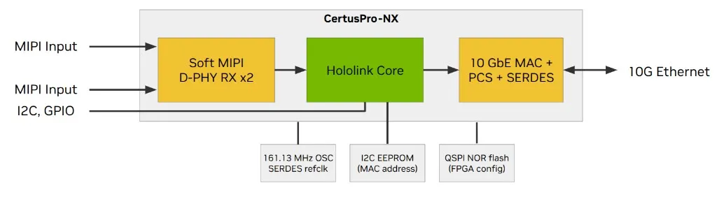
Figure 1. MIPI CPNX Reference Design hardware / FPGA IP block diagram
The MIPI CPNX Reference Design centers on a CertusPro-NX FPGA that receives one or two MIPI CSI-2 camera inputs, processes the sensor data through the Holoscan Sensor Bridge IP, and exchanges data with a host over a 10 GbE link. The FPGA bitstream contains three main functional blocks:
- Soft MIPI D-PHY RX ×2 — receives up to two independent 4-lane MIPI CSI-2 inputs using Lattice soft D-PHY IP.
- Hololink Core — the Holoscan Sensor Bridge IP; packetizes sensor data, handles control-plane traffic, and manages peripheral interfaces (I2C, GPIO).
- 10 GbE MAC + PCS + SERDES — provides the bidirectional 10 GbE host interface for sensor data egress and control-plane traffic.
The block diagram above shows the FPGA internals and the external hardware connections required by the design.
FPGA inputs and outputs
- MIPI Inputs (×2) — 4-lane MIPI CSI-2 camera interfaces (Ports 0 and 1).
- I2C, GPIO — control and general-purpose I/O routed to the Hololink Core for sensor configuration and board-level control.
- 10G Ethernet — bidirectional high-speed link to the host over an SFP+ interface.
See Suggested BOM below for the required external components and suggested part numbers.
Reprogramming the lane count and clock rate
If you wish to use the design with 1- or 2-lane sensors, or use a different clock range, you can reprogram the MIPI Soft DPHY registers from Python or C++ without modifying the FPGA bitfile. Here is an example Python function to do this:
Source Files
The FPGA source code for the project is located in the Holoscan Sensor Bridge repository
at fpga/nv_mipi_ref_design/mipi_cpnx_ref_design. The pre-built bitfile is located
here.
Reference Hardware
You can use the MIPI CPNX Reference Design on supported hardware. The current hardware platforms that supports this design include the Tauro Technologies DA326 Holoscan GMSL adapter.
We have several examples that illustrate the DA326 connected to a
Leopard Imaging Hawk camera
in the repository’s examples directory; these have the name “hawk” in them. These can
be modified to support different GMSL2 cameras or raw MIPI sensors with your own
hardware.
Custom Hardware
Developers can use this design (including the prebuilt bitfile) in custom hardware designs built around the Lattice Semiconductor CertusPro-NX device. Consult Lattice documentation (especially the CertusPro-NX Hardware Checklist) when working with the part — paying special attention to the power topology for the SERDES block.
To ensure 100% bitfile compatibility with your reference design, please use the following design constraints when designing your PCB.
Suggested BOM
The following external components are required for a bitfile-compatible implementation of this reference design.
Equivalent parts may be substituted provided they meet the electrical and timing requirements described in the pin tables below.
Banks and Voltage Rails
10 GbE host interface
MIPI CSI-2 receive — Port 0
MIPI CSI-2 receive — Port 1
Sensor & power control
I2C buses
QSPI configuration flash
GPIO
These GPIO signals can be direction runtime-configurable and used for any application; defaults shown below:
Note: on the Tauro Technologies DA326, GPIO[0] is used as the enable signal for the PoC controller, and GPIO[1] is used as the INT signal for this chip.